• Blog

Embedded Touchscreen Surface Treatments: Elevating User Experiences and Functionality

Today, touchscreens are an integral part of daily life. From cooking equipment and various control units to dental office sterilization machines and automotive displays, these intuitive interfaces have revolutionized how we interact with technology.

As embedded touchscreens have evolved, so too have the challenges associated with their surfaces. Glare, fingerprints, and bacteria are just a few of the issues that can hinder the user experience. However, advanced surface treatments are an innovative solution to these issues that improve both the aesthetics and functionality of the touchscreens they are applied to.


Treatments, Films & Overlays for Superior User Experiences

At e2ip, we perform a variety of human-machine interface (HMI) treatments to promote more efficient, safe and reliable user experiences (UXs):

Anti-Reflection (AR) Coating: Enhance Optical Clarity

When it comes to human-machine interfaces, clarity is a must. The problem is that your display is typically a reflective surface. Anti-Reflection (AR) coatings or films, however, offer a practical solution to this age-old problem. By applying a thin film or coating to the front surface of the glass surface of the LCD display, these treatments filter or cancel out reflections and enhance optical clarity. 

Anti-Glare (AG) Coating: Reduce Distractions

In environments where ambient light sources can impede visibility, such as outdoors or under bright indoor lighting, Anti-Glare (AG) treatments come to the rescue. Employing an etching process, AG treatments impart a matte finish to the front surface of the glass lens. 


This simple yet effective solution reduces the adverse effects of reflected images or light sources on the screen surface. This treatment allows users to interact comfortably with your displays without distractions caused by glare.

Anti-FingerPrint (AF) and Anti-Smudge (AS) Treatments: Clean and Clear Displays

Fingerprints and smudges are a nuisance to touch surfaces: they not only affect the aesthetics of the interface, but the user-experience as well. Our Anti-finger print (AF) coating and Anti-smudge (AS) treatments and coatings address this issue head-on. 


By creating an ultra-smooth surface on the glass lens, these treatments minimize the adhesion of oily residues, making fingerprints and smudges a thing of the past. The smooth surface also reduces finger friction, which makes it even easier to navigate the screen. With cleaner, clearer screens, users can interact effortlessly with touch interfaces across various industries.

Anti-Shatter (AS) Film: Improved Durability

In settings like medical facilities or industrial environments, where shattered screens are a safety concern and an operational risk, our Anti-Shatter (AS) films are an effective answer. Applied as a coating, these films prevent the dislodging and spread of glass fragments upon impact or damage to the glass lens or LCD screen. Through enhanced durability AS films provide the peace of mind needed for smooth operations.

Anti-Microbial (AM) Defense: Better Hygiene and Sanitation

Combating microbial contamination is essential for applications where hygiene and sanitation are non-negotiable. That’s why we’ve designed our Anti-Microbial (AM) films to be a proactive defense against harmful bacteria on touchscreen surfaces. By incorporating custom antimicrobial overlay layers, these films allow the treated surface to destroy certain bacterial strains on contact, thus minimizing the risk of cross-contamination. With antimicrobial agents integrated into the overlay film, touchscreens maintain their mechanical performance while upholding stringent hygiene standards.

Textured Treatments: Tactile Feedback

Smooth touchscreen surfaces offer a sleek aesthetic, but they can lack the tactile feedback that our  tactile membrane switches and other systems with physical buttons provide. This is where textured treatments come into play. By incorporating microtextures on the surface, these treatments enhance tactile feedback, giving users a sensation akin to physical buttons. Industries requiring precise inputs can benefit from the improved usability and engagement that textured surfaces offer.

Dead Fronts: Aesthetics and Privacy

In certain scenarios, discretion and aesthetics are of utmost importance. Dead front technology, like the one we have integrated in our capacitive touch switches, caters to these needs by concealing the display until it is activated. This not only enhances aesthetics by presenting a sleek, unobstructed surface but also adds a layer of privacy. Dead fronts find applications in environments where information needs to be revealed selectively, providing both practicality and a modern aesthetic.

e2ip – Expert Touch Surface Technology

Here at e2ip, our proficiency with touch surfaces is testament to our relentless pursuit of enhanced user experiences and device longevity. From preventing glare and smudges to improving hygiene and tactile feedback, these treatments reshape the way users interact with human machine interfaces in a wide variety of applications.

As you consider the diverse array of touch surface treatments available, remember that investing in these advancements not only elevates user experiences but also extends the lifespan of your devices.

As a leader in the field of Smart Structural Surfaces (TM), e2ip technologies continue to drive innovation, offering businesses the tools to create robust, durable and highly functional human machine interfaces. 

Contact us today to get your project started. 

User Interface Selection Guide

At e2ip, our expertise in crafting intuitive user interfaces positions us as leaders in navigating the complexities of switching technologies. With this guide, we delve deeper into the nuances of user interface options, providing you with the knowledge needed to select solutions that not only meet but exceed your business objectives. By focusing on innovation and customization, we aim to enhance your operational efficiency and user satisfaction, ensuring your investment in technology drives tangible results.

Understanding Switch Technologies

Switches and other input solutions have revolutionized how we interact with devices. As the applications for these technologies have increased, so too have the types of switches. From resistive touch and capacitive touch to tactile membranes and beyond, each solution offers distinct features that shape user experiences. 

Factors Influencing User Interface Selection

The success of your product and the quality of the user experience hinges on selecting the right technology. Touch type, tactile feedback, size, accuracy, resolution, response time, clarity, life expectancy, resistance, and ergonomics all play a role.

Evaluating Different Interface Technologies

Here we’ll dive into the specific attributes of some of the most widely used user interface  technologies.

Resistive Touch Technology

Resistive touch screens use layers of conductive and resistive metallic materials. When pressure is applied to the glass panel, these layers connect to determine touch points. This technology offers affordability and resistance to surface contaminants, making it suitable for various environments. 

Its simple construction allows for touch activation with any number of rigid input devices or sources, from fingers to gloves, to styluses and more. Despite their cost-effectiveness, resistive touch surface switches exhibit a moderate level of image clarity—typically around 70% to 85%.

Capacitive Touch Technology

Capacitive screens rely on measuring disruptions in electrical current caused by touch. Transparent electrodes are placed on a glass substrate to detect touch points. These screen surfaces provide high image clarity, scratch resistance, and responsiveness to conductive objects, which is why we have made a point to leverage this technology in the creation of our various capacitive touch interface solutions.

A capacitive touchscreen can be operated using a human skin touch or a stylus holding an electrical charge. They offer excellent clarity with light transmission averaging at 80% or above.

Tactile Membrane Switches

Tactile membrane switches are renowned for their seamless integration as Human Machine Interfaces (HMIs). They embody a harmonious blend of functionality and flexibility. Featuring a simple yet highly customizable design, these switches comprise a circuit layer, a spacer layer, and pressure-sensitive adhesives, all encapsulated between a durable base and a protective top layer. Membrane switches are particularly well-suited for environments where durability, portability, ease of cleaning, and sanitation are important. With sharp tactile feedback, they also offer an unmatched user experience, making them ideal for applications requiring intuitive operation and reliable performance.

Smart Structural Surfaces™

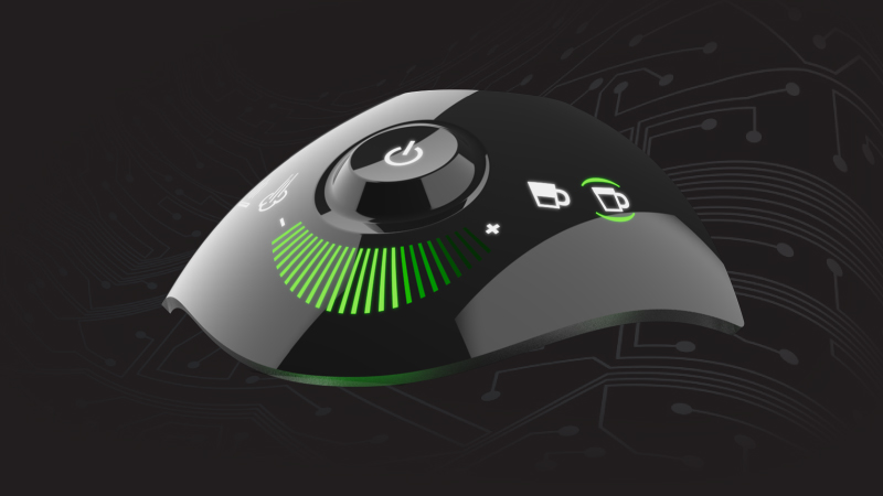
Smart Structural Surfaces™, integrate in-mold electronics (IME) with intuitive designs to create sleek interfaces that enhance the user experience. Providing greater design freedom than other user interface options, they also offer improved reliability, and enhanced touch performance. This cutting-edge technology allows for the creation of smart, curved, and freeform surfaces that blend beautifully into their environment. 


Smart Structural Surfaces™ are a major step forward in smart HMI technology that is driving the future of user experience and opening doors to unprecedented possibilities. 

Tailoring User Interface Selection to Business Needs

Selecting the right user interface technology involves aligning it with specific business applications. Different industries, such as industrial, aerospace, medical, and control systems, each have unique requirements. 

Factors like the environment, user interaction patterns, and deployment conditions significantly impact user interface and switch selection. When it comes to making switch technology decisions for your business, seeking out advice from our experts ensures your solution is tailored to your needs.

Creating the User Interfaces of the Future

The world of switch technologies is full of options for different business needs. By choosing the right switches and interfaces, companies can improve user experiences and productivity. 

As technology continues to develop and permeate the modern business landscape, having effective means of interacting with the devices and machines we use becomes all the more important. Our team here at e2ip is committed to providing businesses with the solutions they need to thrive, whether it’s a switch solution, one of our Smart Structural Surfaces™, or any technology in our offering. Contact us today to learn more! 

Applications and Methods for Fine Line Printing

In the ever-evolving landscape of electronics manufacturing, the demand for smaller, sleeker, and more functional devices has reached new heights. Meeting these demands while maintaining high quality and performance standards has become a top priority for manufacturers.

One of the key innovations that have enabled the creation of such devices is fine-line printing, a process that allows for the creation of incredibly thin and precise conductive lines. In this paper, we will explore various methods for fine-line printing and their applications, offering insights into how these methods are revolutionizing the way we interact with electronic devices.

Fine Line Screen Printing: The Powerhouse of Electronics Manufacturing

Screen printing has long been recognized as a cost-effective method for producing a wide range of electronic components. Its versatility and reliability screen printing remains a preferred choice for many manufacturers. When it comes to fine line printing, screen printing plays a crucial role in achieving precise conductive lines.

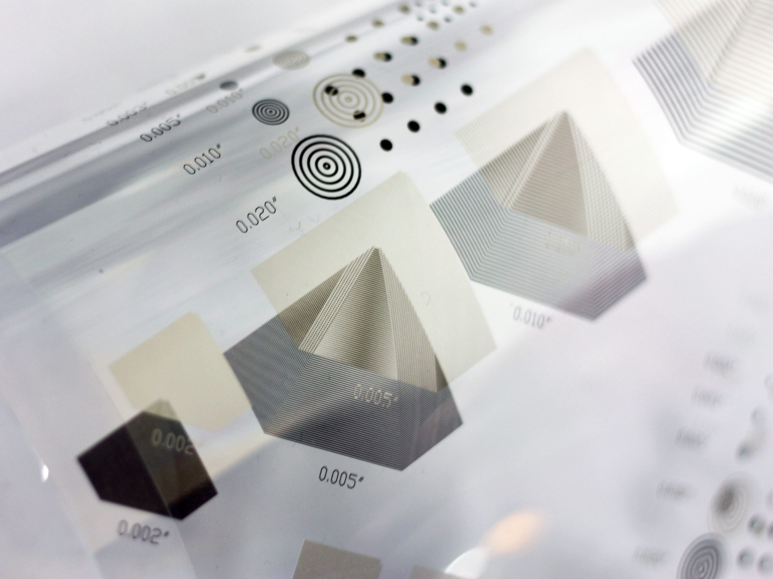
Fine line screen printing leverages the thinness of wire meshes to create conductive lines as narrow as 50µm or even narrower. This method is particularly suitable for applications requiring high-resolution conductive patterns, such as solar cells, touch panels, and low-temperature co-fired ceramic (LTCC) electrodes.

Calendered Wire Mesh: Enhancing Performance

Calendered wire mesh is a process that enhances the performance of screen printing in several ways. By flattening the mesh using the high-pressure rollers, this method stabilizes the mesh structure, leading to improved dimensional accuracy. The flattened knuckles of warp and weft wires result in a thinner paste deposit and smoother surface, contributing to better print resolution. 

Hybrid Solutions: Combining Screen Printing and Laser Patterning

Hybrid solutions combine the strengths of screen printing with laser patterning to achieve fine-line printing with extreme dimensional accuracy. This method is particularly valuable for applications like touch screen edge electrodes, where complex patterns demand precise and repeatable results from both the screen and printing machine.

Direct Ultra-fine Line Printing: Pushing the Boundaries

Direct ultra-fine line printing is at the forefront of fine line printing technology, pushing the boundaries of what is possible. This method involves wire meshes with wire diameters as thin as 20µm, high-resolution emulsion, and glass masks, resulting in extremely fine conductive lines. Applications for this technology include TFT backplane metallization, transparent RFID antennas, and printed electronics sensors.

Offset-Based Printing: A Smoother Approach

Offset-based printing offers a smoother approach to fine-line printing by embossing fine grooves into the substrate and then filling them with conductive ink. This method provides precise and smooth conductive lines, and the depth of the grooves can be adjusted to achieve higher conductivity levels without compromising line width. It is particularly well-suited for large-area transparent heating applications.

Pushing the Limits with Fine Line Printing

As technology continues to advance, the methods for fine-line printing are constantly evolving. Advances in screen printing, hybrid solutions, and direct ultra-fine line printing are pushing the limits of what can be achieved in electronics manufacturing. These methods are opening doors to new applications and revolutionizing industries such as solar cells, touch panels, and flexible electronics, and we at e2ip are committed to being at the forefront of these developments.

e2ip – Your Partner in Precision Fine Line Printing Solutions

Fine-line printing is a cornerstone of modern electronics, enabling the creation of smaller, more advanced components. e2ip‘s expertise and dedication to innovation make us a trusted partner for companies seeking to leverage solutions such as fine-line printing, conductive inks for printed electronics, and more. We encourage you to explore the vast potential of fine-line printing– e2ip technologies is here to help you from ideation to fabrication. 

HMI Design Guidelines for Industrial Applications

In today’s modern industrial settings, Human Machine Interface (HMI) plays a crucial role as the bridge between humans and machines in control systems. A well-designed HMI can significantly impact operator experience, productivity, and overall operational efficiency. 

At e2ip technologies, we recognize the importance of effective HMI solutions and are committed to delivering innovative and user-friendly interfaces that empower industries to thrive.

Understanding Human Machine Interface (HMI)

An HMI serves as the essential interface through which operators interact with machines and processes in control systems. Its significance lies in the seamless exchange of information, allowing humans to monitor and control complex industrial operations. Well-designed HMIs ensure a user-friendly and efficient experience for operators, ultimately leading to improved productivity and safety.

Key Components of HMI Screens

HMI screens are composed of various elements that collectively form an intuitive and informative interface. Clicktouch technology enables operators to interact effortlessly with the system, while dynamic graphics provide real-time feedback. HMI screen design features for displaying data effectively, such as line graphs and trend objects, allow operators to grasp critical information at a glance, enhancing situational awareness.

Guidelines for Designing Effective HMI Screens

Light Gray Screen Background and Color Usage

Utilizing a light gray screen background is a design choice that reduces visual clutter and enhances readability. Thoughtful color usage helps convey information effectively and avoids distracting the operator. When used judiciously, colors and animations can aid in highlighting essential details without overwhelming the user.

Consistent Screen Menus and Navigation

Consistency in screen menus and navigation is paramount for an HMI’s ease of use. Ensuring quick access to essential functions streamlines operator workflow and enhances overall efficiency. The incorporation of a background screen maintains consistency throughout the application, creating a seamless user experience.

Dynamic Graphics and Effective Data Display

Dynamic graphics are a powerful tool in HMI screens, providing operators with intuitive visual cues and real-time status updates. Proper data displays on equipment status screens empower operators to monitor trends and predict potential issues promptly.

Reserving Space for Important Items

Dedicating a portion of the screen to critical information, such as start/stop buttons and key set points, ensures essential data is readily available to operators. Organizing screen elements thoughtfully optimizes operator interaction and workflow, contributing to an efficient and user-centric design.

Engaging Operators and User Feedback

Talking to Operators and Gathering Input

Engaging with operators during the HMI design process is essential to understand their specific needs and tasks. Storyboards serve as valuable tools to gather feedback, ensuring that the design aligns with operator requirements and preferences, especially when a certain operation involves the use of both primary and alternate screens or interfaces.

Using Images and Real-world Visuals

Incorporating relevant images and real-world visuals aids operators in understanding machine status at a glance. Striking a balance between conveying essential information and avoiding excessive detail is crucial in creating clarity and enhancing user comprehension.

Leading the Operator and Providing Feedback

Color and animation can guide operators through complex processes and provide affirmative feedback for task completion. Ensuring situational awareness by displaying pertinent information concerning the current state of the machine or process further enhances operator performance.

Optimization and Standardization

Limiting Screen Access Clicks and Complexity

Minimizing the number of clicks required to access screens and optimizing the HMI layout streamline operator workflow and efficiency. Reducing complexity and providing clear navigation paths contribute to a smoother and more productive user experience.

Developing Style Guides and Object Libraries

Creating style guides promotes consistent HMI design across multiple screens, projects, and facilities, enhancing operator familiarity. Object libraries facilitate the efficient reuse of common elements, optimizing design and development time for HMIs.

Empowering Companies Through Innovative HMI Solutions

Designing effective HMI screens with a focus on interface and graphics is paramount in modern industrial settings.

A well-crafted HMI empowers operators, improves productivity, and optimizes control systems. At e2ip technologies, we take pride in our expertise in HMI solutions, smart structural surfaces, and innovative user interfaces that enable companies to achieve their goals.

With a commitment to excellence, we create HMI designs that redefine the way industries operate and thrive.


Fine Line Technology For Capacitive Touch Sensors

e2ip technologies can create the functional layers of a Transparent Capacitive Switch (TCS) circuit using our production scale Screen Printing facilities. Conductive materials like our MINK or commercially available conductive pastes allow us to screen print <30-micron resolution of transparent metal mesh electrodes. The inks are printed on commercially available PET substrates and high-quality screens.

High-resolution emulsion Technology and Advanced Stainless Steel meshes allow for better edge definition and ultra-fine resolution (10-30 microns below).

PET Substrate technology has also improved to help in the areas of Adhesion, Temperature Dissipation, preventing Paste Spread, and obtaining Smaller Feature sizes (see below).

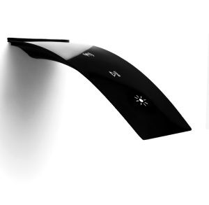
The design, manufacture, and assembly of this switch is done at e2ip technologies. Screen printed TSC circuit is adhesive bonded to LED circuit for backlighting the icons, light guide film and finally to a dead-front graphic label to make a thin and curved control panel demonstrator with single and multi-touch capability. The backlighting of the icons can be activated by touching the specific area.

Applications like Human Machine Interfaces (HMI) for automotive, home appliances, medical, and aerospace markets are driving this development. Flexible transparent capacitive switches enable a high level of differentiation and design freedom to make thin, ergonomic, and functional surfaces with attractive backlit schemes.

Being sensitive to the manufacturing costs, we consider individual Screen-Printing cycle times of 3-6 seconds for a single pass to help reduce overhead costs. Faster Takt times (the rate at which you need to complete a product to meet customer demand) are possible thanks to the manufacturing speeds of our current processes.

Screen-printed TCS designs provide a more reliable, more cost-effective, and more environmentally friendly solution than conventional electronics (i.e., copper flex), all of which are the key drivers and trends in the above-mentioned markets.

By reducing feature size and layer thickness, e2ip technologies can produce the devices of the future. Printed Electronics know-how and the use of the latest Mesh Technology, Emulsion Technology, Paste Technology, Substrate Technology, and our Professional Screen-Printing manufacturing allow us to produce Advanced IME Devices.

We want to thank our vendors for supporting us during the development of this Transparent Capacitive Switch: 

  • Sun Chemical 
  • Asada Mesh 
  • Sefar US 
  • Kiwo 

How to Secure Embedded Systems: A Short Guide to Cyber Security for Embedded Systems

Embedded systems have become an integral part of various industries, powering everyday devices and enabling advanced applications in industrial settings. These compact computing systems play a crucial role in modern technology, but they also pose unique security challenges. As the reliance on embedded systems continues to grow, the need for embedded systems security becomes paramount to protect sensitive data and ensure reliable operation.

In this article, we will explore the key aspects of securing embedded systems and the best practices to implement. As a leading provider of Smart Structural Surfaces™,e2ip technologies is committed to delivering secure embedded systems that meet the highest industry standards.

Understanding Embedded Systems and Their Security Challenges

Embedded systems are specialized computing devices designed to perform dedicated functions within larger systems. They are commonly found in household appliances, medical devices, automotive electronics, and more. Unlike general-purpose computers, embedded systems are tailored for specific tasks, offering efficiency and compactness.

Key Security Challenges in Embedded Systems

Securing embedded systems presents unique challenges due to their resource constraints and diverse applications. One critical aspect is power consumption, as optimizing power usage can impact security. The team at e2ip technologies recognizes these challenges and works to develop secure embedded systems that prioritize both efficiency and protection.

Best Practices for Building a Secure Embedded System

Implementing Strong Authentication and Authorization Mechanisms

Authentication plays a crucial role in ensuring that only authorized users can access the embedded system. Implementing robust authentication and authorization mechanisms prevents unauthorized access and potential data breaches.

Address Space Layout Randomization for Improved Security

Address Space Layout Randomization (ASLR) is a security technique that helps protect embedded systems from memory-based attacks. By randomizing memory locations, ASLR makes it difficult for attackers to predict where specific data or functions are stored, thus enhancing overall security of the system and its embedded devices.

Leveraging Trusted Execution Environments

Trusted Execution Environments (TEEs) provide a secure area within an embedded system’s processor. TEEs protect critical processes and sensitive data from unauthorized access or tampering.

Containerization of Software Applications

Containerization isolates software components, enabling enhanced security by limiting the potential impact of a breach to a specific container.

Selecting a Secure Embedded Operating System

The choice of an embedded operating system significantly impacts the security of the entire system. Selecting a secure operating system is crucial to prevent potential security vulnerabilities and ensure the long-term stability of the embedded system. When selecting an operating system, it is essential to consider the embedded security features and their integration capabilities.

Power Management Techniques for Enhanced Security

Power efficiency is a critical consideration in embedded systems, as it impacts both performance and security. At e2ip technologies, we excel in power management techniques and ensure products like our smart Touch Surfaces devices deliver reliable operations while conserving energy. 

Power-efficient software development also plays a vital role in maximizing the performance and longevity of embedded systems. It’s important to select embedded systems that are designed based on reliable software development practices that reduce power consumption without compromising on security or functionality.

Partner with e2ip technologies for Unrivaled Embedded System Security

Securing embedded systems is of paramount importance in today’s interconnected world. Understanding the unique challenges and implementing best practices are essential to safeguard sensitive data and ensure reliable operation.

Companies can trust e2ip technologies to deliver secure smart surface solutions, innovative electromechanical systems, and robust embedded systems that leverage our expertise to stay at the forefront of embedded system security. By partnering with e2ip technologies, you can confidently embrace the power of embedded systems without compromising on security.

Benefits of Early Engagement and Collaboration in the Development of Custom HMI Solutions

When creating human machine interface solutions, success hinges on more than just advanced technology and sleek design. It’s about the art of collaboration – the vital synergy between visionaries, developers, and end-users that brings exceptional HMIs to life.

At e2ip technologies, we firmly believe that the best human machine interfaces are born through collaboration at the ideation and conceptualization stages. By emphasizing the importance of early collaboration, we ensure that both customers and end-users receive HMI solutions that exceed expectations and shine bright in their respective applications.

Let’s explore the benefits of this collaborative approach and uncover how it leads to HMI excellence.

What is HMI Development?

HMI development refers to the art and science of crafting human machine interface (HMI) solutions. As a leading expert in this field, we specialize in creating intuitive and cutting-edge Smart Structural Surfaces™ that bridge the gap between humans and machines.

At e2ip technologies, our collaborative approach ensures that each HMI solution is tailored to the specific application, delivering outstanding performance and positive user experiences. Let’s take a closer look:

Better Design & Development Decisions: A Journey of Informed Choices

The journey to creating excellent HMI systems starts with well-informed decisions. Early collaboration brings all stakeholders together, enabling a comprehensive understanding of project requirements, restrictions and time frames.

Leverage Expertise & Knowledge

When it comes to HMI design, experience is a priceless asset. With early collaboration, our team of experts becomes an extension of our customers’ vision. Leveraging our accumulated knowledge and expertise, we make informed design decisions that optimize HMI solutions for specific applications.

Our collaborative approach fosters a seamless exchange of ideas, ensuring that each project is enriched with our years of experience. Together, we create HMI designs that surpass expectations and elevate user experiences.

Finding the Best Solutions for Each Application

We understand that every HMI application requires a bespoke approach. Early collaboration allows us to delve into the specific needs of industrial processes or end-user experiences, ensuring that our HMI system solution aligns perfectly with the intended application.

e2ip’s Smart Touch Surfaces revolutionize HMI experiences, taking interactivity to new heights. With touch capabilities, they provide seamless interaction, delivering intuitive and efficient control systems. Whether in medical devices, industrial control panels, or consumer electronics, smart touch surfaces enhance functionality and aesthetics, making them the preferred choice for modern HMI solutions.

When it comes to HMI programming and software, delivering exceptional end-user experiences requires a thoughtful and user-centric approach. We prioritize intuitive interface design, ensuring smooth navigation and seamless interactions. Our experienced HMI programmer team creates responsive and user-friendly control systems.

By focusing on usability and visual aesthetics of HMI screens, we craft interfaces that captivate users and enhance their overall experience. Regular testing and iterative improvements further refine our HMI software. Our approach lies in understanding users’ needs, designing with empathy, and continuously refining our HMI solutions for unparalleled end-user experiences.

Reducing Risks

Early collaboration is a catalyst for accelerating the design and development process, ensuring swift and efficient progress, as the HMI creation process is not without uncertainties.

By engaging with e2ip from the outset, potential material availability or supply chain challenges are identified proactively. Our contingency plans and strategic measures ensure seamless execution, mitigating potential disruptions and delivering HMI solutions that are on time and on point.

This efficient exchange of information lays the groundwork for seamless project execution and clear progress tracking.

Identify & Seize Opportunities for Innovation & Design Optimization to Perfect the End-Use Experience

Innovation thrives in a collaborative environment. Early engagement encourages the exploration of new ideas and technologies, uncovering opportunities for innovation and design optimization.

Precision is paramount in HMI development. Early collaboration allows e2ip technologies to optimize product design and materials selection, ensuring that the final HMI solution perfectly aligns with its intended application, delivering an unparalleled end-user experience.

Improved Problem-Solving & Issue Resolution

It is often said that prevention is better than a cure, and this rings especially true in HMI development. By addressing potential issues early on, we minimize the need for rework and ensure a smooth project progression.

For example, harsh environments pose particular difficulties for effective HMI development. If environmental or use case challenges are identified early on, the design can move away from traditional mechanical switches or capacitive solutions to incorporate ClickTouch™ technology.  This proprietary advanced membrane switch technology from e2ip, reduces parts, enhances durability and provides extended key travel for improved tactile feedback. With dust, dirt, and water-tight properties, ClickTouch™ excels in harsh environments, offering a reliable and long-lasting user experience.

In a competitive market, time is a precious commodity. Early engagement leads to reduced implementation time and enhanced efficiency, delivering HMIs that reach the market faster.

Embrace the Power of Early Collaboration

Collaboration is the cornerstone of HMI excellence. By initiating collaboration at the ideation and conceptualization stages, e2ip technologies ensures that HMI solutions surpass expectations and shine brightly in their respective applications. The benefits of early collaboration span from better design decisions to reduced risks and enhanced end-user experiences.

Are you ready to embark on this collaborative journey with us? Embrace the power of early collaboration and unlock the full potential of your HMI projects with e2ip technologies. Contact us today!

Exciting Opportunities for Printed Electronics and Printed Sensors in Future Medical Applications

The printed electronics industry has existed for decades, and today, printed electronics are commonly found in almost every modern device. Their lightweight, compact, and flexible design contributes to their widespread adoption across various industries. Additionally, cost-effective manufacturing techniques have made them ubiquitous to the extent they have become almost invisible and often go unnoticed, yet they continue to play a crucial role in introducing and enabling new functionalities, improving product quality, and enriching user experiences.

The industry is once again experiencing a resurgence due to recent innovations and material advancements, leading to new and exciting possibilities, while concurrently elevating and improving existing technologies. One notable advancement is Printed Sensors, which represents a natural progression in this field.  Printed sensors seamlessly integrate sensing capabilities directly onto or into electronic devices to detect a wide range of physical and chemical parameters. Their versatility unlocks endless opportunities for innovative solutions in medical, healthcare and fitness applications, offering cost-effective sensor solutions that can be tailored for various use cases.

Biosensors vs Biometric Sensors

In the context of printed sensors used in medical devices and healthcare applications, it is important to understand the fundamental difference between biometric sensors and biosensors. Although both sensors share similarities, their underlying principles and applications are different and distinct.

Biometric Sensors:

Biometric sensors serve the primary purpose of capturing and analyzing unique human and physical characteristics, typically for identification or authentication purpose.  These sensors capture and analyze specific biometric data, such as fingerprints, facial features, iris patterns, or voice patterns, and use this information for user identification or verification. Biometric sensors are commonly used in access control systems, identification processes, and security applications.

Biosensors:

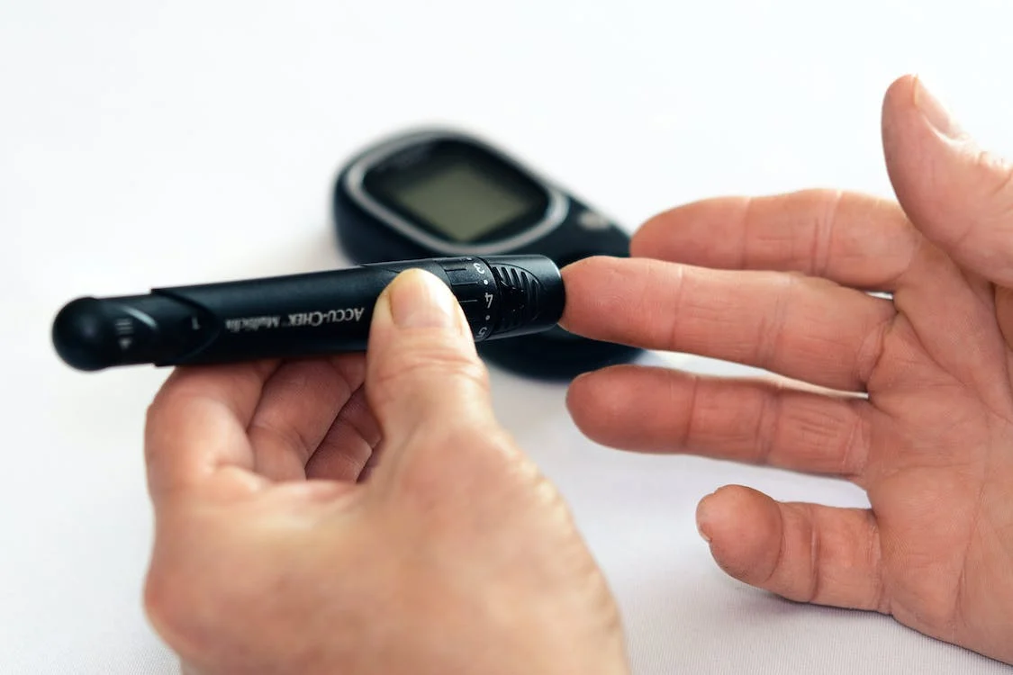
Biosensors are analytic devices that convert a biological or physiological response or marker into an electrical signal.  Biosensors can be external in nature, such as the glucose strip of a glucose monitoring device, or they can be attached or worn on the human body and are commonly integrated into wearable devices for continuous health monitoring and tracking.

Examples include ECG sensors, which measure and monitor a heart’s electrical activity, EEG sensors which monitor brain activity, and biological sensors that are capable of measuring and monitoring biological substances for biomarkers such as glucose, cholesterol, pH levels, proteins, or pathogens.

Although biosensors are typically non-invasive in nature, they can be designed as implantable devices that offer unique advantages for long-term monitoring capabilities, thereby expanding their potential applications in healthcare.

Despite their differences, the terms “biometric sensors” and “biosensors” are often loosely interchanged because they both involve biological signals and measurements.  However, it is important to be precise and contextually aware when using these terms to avoid unnecessary confusion.  For the sake of clarity and consistency in this context, we will use the term ‘biosensor’ to refer to sensors that detect and measure specific biological or physiological parameters for diagnostic and monitoring purposes in healthcare.

Changes in Healthcare and the Medical Industry
A Not-So-Distant Scenario

Imagine this scenario: A man is cycling in the park when his wearable sensor detects early signs of a potential stroke, triggering an instant alert. Simultaneously, the information is sent to both his personal AI provider and his family. The AI promptly analyzes the data and administers life-saving medication through a conductive printed patch, which the man already carries for such emergencies.

At the same time, his family receives the notification and acts promptly to offer support and assistance. They have the option to either call for emergency services or rush to his location to be by his side and provide support and assistance. Alternatively, depending on the severity of the event, the man can opt for a nearby solution by riding just 5 minutes to his local pharmacy to get a refill of the printed patch.

This scenario illustrates the immense potential of cutting-edge technology, including wearable biosensors, AI algorithms, and printed electronics, in transforming healthcare and emergency response. With real-time monitoring, quick analysis, and timely interventions, such innovations are poised to improve outcomes and save lives.

The introduction of telehealth and telemedicine marked the beginning of effective outpatient healthcare solutions, enabling remote consultations & medical services outside the traditional healthcare setting.  Similarly, the introduction of EMR (Electronic Medical Records) revolutionized how medical data is collected, recorded & stored, with significant benefits in downstream studies and analytics to help aid in identifying patterns, trends and correlations in patient data and predicting outcomes.

The healthcare industry continues to change and evolve and is now making a transformative shift towards “Smart” and connected solutions, driven by a growing need for real-time and remote monitoring in outpatient settings. This shift involves the integration and use of cutting-edge technologies such as Artificial Intelligence (AI), virtual assistance, Internet of Things (IoT), NFC, and wireless networking and communications, and printed electronics and sensors. These advancements hold the potential for profound implications in patient care, not only within medical facilities but also in the realm of in-home healthcare.  With mounting strains and challenges on already limited resources, healthcare facilities are actively exploring various options to reduce and mitigate burden and waste, to help optimize healthcare diagnostics and treatment delivery, and to create a more responsive, resilient, and efficient healthcare system that ultimately improves patient treatment and outcomes.

The Potential of Printed Electronics and Printed Sensors
Printed electronics is an innovative and continuously evolving and advancing technology that has revolutionized the design and production of medical devices and sensors. Recent breakthroughs have significantly contributed to the advancement of printed sensors in medical applications:

Fine-line Printing:  Advanced printing methods and capabilities can achieve ultra-fine printing resolution has enabled the creation of intricate and highly precise sensor patterns. Fine-line printing techniques can improve the accuracy and sensitivity of sensors, making them more suitable for detecting subtle changes in physiological parameters.

Functional Inks: The development of specialized functional inks has expanded the range of sensing capabilities. For example, conductive inks with enhanced biocompatibility and biodegradability have enabled the integration of sensors directly onto or into the human body without causing adverse reactions.  Molecular inks can be formulated to offer specific properties and functionalities such as improved sensitivity and accuracy, or to react to specific biological substances or biomarkers.

Transparent Inks:  Allows for the creation and printing of near-invisible, discreet wearable devices that can be applied directly to the skin without being visibly intrusive, which patients can wear without feeling sub-conscious.  Additionally, transparent inks are well suited for integration into sensors requiring optically clear or transparent/translucent properties, such as heart rate monitors, oxygen saturation sensors, or imaging sensors.

Flexible and Stretchable Substrates:  Printing sensors on flexible and stretchable substrates allows them to conform better to the curved shapes of the human body. This innovation has led to the creation of wearable sensors that are comfortable to wear and unobtrusive.

Multi-Modal Sensing: Advanced printed sensors can now detect multiple parameters simultaneously, offering multi-modal sensing capabilities. For instance, a single sensor may measure both temperature and pressure, providing a comprehensive assessment of a patient’s condition.

Wireless Communication: Printed sensors with wireless communication capabilities can transmit real-time data to healthcare providers, enabling remote patient monitoring. This breakthrough has enhanced telemedicine applications and improved patient care, especially in remote or home-based healthcare settings.

Hybrid Integration: Printed electronics can now be seamlessly integrated with other components, such as microcontrollers or batteries, enhancing the overall functionality of printed sensors. This integration enables the development of more sophisticated and versatile medical devices.

The continuous advancements and breakthroughs in printed electronics and sensors have significantly enhanced their potential and applications in the medical industry. As a result, there is a growing adoption of printed electronics and sensors in healthcare, benefiting from their versatility and customizable form factors. These advancements offer many advantages, including quicker detection and diagnosis, improved accuracy and reliability of sensor data, enhanced patient comfort and convenience, self-monitoring capabilities, and cost reduction across the healthcare ecosystem.

One area where printed sensors have had a significant impact is in the development of inexpensive, flexible, and wearable technologies. These lightweight devices can be directly applied to the skin or seamlessly integrated into clothing, enabling various medical applications such as therapies, medicine delivery, and continuous monitoring. The ability to print sensors on flexible and stretchable substrates allows them to conform better to the curved shapes and repeated movements of the human body, making them comfortable for long-term wear.

Moreover, printed sensors can be designed for either long-term use or as disposable applications, with the latter being extensively used in healthcare facilities to reduce infection risks and prevent pathogen transmission. The materials used in disposable sensors are non-toxic and easily biodegradable, making them both cost-effective and environmentally sustainable.  Additionally, materials can be enhanced with anti-microbial properties, providing an added layer of protection, and enhancing both patient and caregiver safety.

Sensors play a crucial role in monitoring various physiological parameters like heart rate, temperature, blood pressure, and respiratory rate. Their integration into medical devices and implantable solutions improves patient care, diagnosis, and overall health monitoring in a cost-effective and sustainable manner.

The continuous progress in printed sensor technology is driving a revolution in the medical industry, paving the way for innovative and efficient healthcare solutions. The future holds even more promising innovations that will further transform the medical sector, providing improved healthcare solutions and enhancing patient well-being. Additionally, the convergence of printed electronics and sensors with other state-of-the-art technologies like In-Mold Electronics (IME) will unlock new possibilities and opportunities for growth and advancement in medical devices and healthcare solutions.

Reliable Sensors – Key to Quality Medical Treatment

The design and manufacturing of printed sensors requires multi-disciplinary knowledge and expertise across various disciplines.  Additionally, the design and manufacturing of accurate  and reliable printed sensors relies on several key aspects:

Robust Sensor Design: Creating robust printed sensors requires careful consideration of the unique demands of the intended application. The layout and design of the printed circuit are critical factors influencing the sensor’s accuracy. Key elements like trace width, spacing, pattern and alignment directly impact the electrical conductivity, sensitivity, and signal integrity of the sensor. Additionally, the design must account for the sensor’s long-term reliability and durability, particularly when deployed in real-world medical scenarios, where exposure to diverse environmental conditions or biological fluids is likely. By paying close attention to these design aspects, printed sensors can offer optimal performance and longevity in their intended applications.

Sensor Type and Technology: Selecting and designing the appropriate sensor type and technology is crucial. Printed sensors can come in various forms, including electrochemical sensors, biosensors, strain sensors, and temperature sensors, among others. The choice depends on the targeted application and the parameters to be measured. Additionally, it might be advantageous to design the sensor as multi-model, capable of measuring and monitoring multiple parameters simultaneously.

Material Selection: Choosing the right materials, including conductive inks, substrates, and functional coatings, is essential for sensor performance. The materials should be biocompatible, stable, and capable of maintaining consistent electrical properties over the intended life or usage of the sensor.

Power Consumption: For wearable sensors or remote monitoring devices, low power consumption is critical to prolong battery life and enable extended use without the need for excessively frequent or extended recharging times.

Industry and regulatory Standards :In the design and manufacturing of sensors, it is essential to adhere to all relevant industry and regulatory standards and guidelines. Doing so ensures that the products meet the necessary safety, performance, and quality requirements. By following these standards, manufacturers can produce sensors that are reliable, effective, and compliant with established norms, fostering confidence in their performance and usability.

Algorithms and signal processing: Algorithms and signal processing are essential components in the design of printed sensors. They play a critical role in converting the raw analog signals generated by the sensor into digital information that can be effectively analyzed and utilized for various applications. Raw data often contains unwanted noise and interference, which can negatively impact the accuracy and reliability of the sensor’s measurements. Algorithms are employed to enhance the signal-to-noise ratio, resulting in more precise and dependable readings. By effectively processing the sensor’s signals, algorithms ensure that the data collected is of high quality and can be effectively used for real-world applications.

In the medical industry, additive manufacturing and established printed electronics techniques are used to produce sensors for a diverse range of healthcare applications, resulting in cost-effective sensors and medical device production.  As new technologies and advancements are embraced and integrated, the potential for printed electronics in medical applications continues to evolve and grow.

e2ip’s Role in Medical Printed Electronics Innovation 

Choosing a reputable manufacturer with practical experience, extensive technical expertise, advanced processing capabilities, and a proven track record and reputation of consistently delivering high-quality printed electronics and sensors is crucial.

At e2ip Technologies, we have the qualifications and expertise required to meet your specific membrane switch requirements. With our longstanding presence as an industry leader and a proven history of innovation, we invite you to get in touch with us today and provide details about your project. We are prepared to address any inquiries you may have, and our dedicated team of experts is committed to helping you find the ideal solution that perfectly aligns with your unique needs.

To learn more about how e2ip can support your need, product, or project in any industry, contact us or call us in the Montreal area at (514) 631-6662 or internationally, at 1-866-631-6662.  

Revolutionizing 5G Network Deployment with 5G Smart Surfaces

The advent of 5G technology promises to bring about a transformative era of unprecedented connectivity and communication. However, the successful deployment and optimization of 5G networks present a series of challenges, including signal propagation, interference, and coverage. To address these hurdles, engineers and researchers are turning to a cutting-edge solution known as Engineered Electromagnetic Surfaces (EES) or 5G Smart Surfaces. In this blog, we will explore how 5G Smart Surfaces can significantly impact 5G network deployment, revolutionizing the way we experience connectivity.

Understanding 5G Smart Surfaces

5G Smart Surfaces, often referred to as electromagnetic metamaterials or metasurfaces, are passive surfaces designed to manipulate and control electromagnetic waves in novel ways. Unlike conventional materials, 5G Smart Surfaces artificially enhance wireless coverage at microwave and millimeter-wave frequencies via printed conductive patterns on substrates such as plastic, wallpaper or glass.

5g-smart-surfaces-e2ip technologies

Enhanced Signal Propagation and Range

One of the critical challenges faced during 5G deployment is ensuring reliable signal propagation and sufficient coverage, especially in urban areas with high-rise buildings and dense infrastructure. 5G Smart Surfaces can play a vital role in overcoming these obstacles. By strategically placing 5G Smart Surfaces near 5G antennas, it is possible to manipulate and redirect the signal propagation in specific directions, thus optimizing the propagation path and extending the range of the wireless signal. This capability translates into better coverage and reduced signal loss, enabling a seamless 5G experience for users across a broader area.

Minimizing Interference and Enhancing Capacity

In densely populated urban environments, interference between neighboring 5G cells can significantly impact network coverage. 5G Smart Surfaces offer a unique advantage in this regard. By tailoring the electromagnetic properties of these surfaces, engineers can create “stealth” materials that can either absorb, redirect, or diffuse the signal in a desired direction effectively either minimizing the adverse effects of signal overlap or enhancing the overall network capacity. This opens new possibilities for densely packed 5G cells, enabling network providers to optimize resource allocation and deliver improved data speeds and user experiences.

Overcoming Obstacles and Line-of-Sight Limitations

Outdoor Demo Video

Indoor Demo Video

5G’s high-frequency millimeter waves have the potential to deliver astounding speeds and low latency, but they are susceptible to obstacles like buildings and foliage. 5G Smart Surfaces can be designed to work as “smart mirrors,” reflecting and bending millimeter waves around obstacles, effectively establishing non-line-of-sight connections. This capability expands the possibilities of 5G network deployment, as providers can establish connectivity in challenging environments where direct line-of-sight transmission may not be feasible.

Energy Efficiency and Reduced Environmental Impact

As the world increasingly focuses on sustainability, energy efficiency in communication technologies becomes crucial. 5G Smart Surfaces can aid in reducing the power consumption of 5G networks. By controlling the electromagnetic wavefronts passively and with precision, these engineered surfaces can optimize signal transmission paths, reducing the need for high-power transmissions. The result is a more energy-efficient network that not only reduces operational costs but also minimizes the environmental impact associated with 5G deployment.

Future-Proofing the Network

5G is just the beginning of our journey towards a hyper-connected world. As we set our sights on future generations of wireless technology, the flexibility and adaptability of 5G Smart Surfaces become invaluable. These engineered surfaces can be designed and configured to support evolving communication standards, ensuring that the network infrastructure remains relevant and capable of seamlessly integrating with upcoming technologies.

5G Smart Surfaces are set to revolutionize the way we deploy and experience 5G networks. From extending coverage and enhancing capacity to overcoming line-of-sight limitations and reducing interference, 5G Smart Surfaces offer a host of advantages that pave the way for a more connected and efficient future. As researchers and engineers continue to push the boundaries of electromagnetic metamaterials, we can expect even more innovative solutions to address the challenges of 5G deployment and future wireless communication technologies. With 5G Smart Surfaces at the forefront of this technological revolution, the future of 5G networks appears brighter than ever before.

With our innovative technology and commitment to advancing the field of smart surfaces, we at E2IP TECHNOLOGIES, seek to apply our many years of experience in the field of electronics, creating technologies like smart touch surfaces and more, to help push this technological revolution forward. Contact us today for more details about our 5g smart surfaces.

In-Mold Electronics (IME): How In-Mold Decorating (IMD) and In-Mold Labeling (IML) are Changing the Game for Designers

In-Mold Electronics (IME), or Smart Structural Surfaces™, promise to be a game-changing technology that will significantly improve process optimization. 

IME provides for a streamlined production process over traditional electronic assembly. Simply put, IME is a three-step process which includes the printing of electronic circuits and graphics, followed by the forming and molding. However, In-Mold Electronics is often confused with related processes, namely In-Mold decorating (IMD) and In-Mold Labels (IML).

What is the Difference Between IML and IMD?

IME’s roots are tied to both IMD and to a lesser degree IML. IME takes the process of printing, forming, and molding to a new level of complexity. Both IMD and IML offer a streamlined process utilizing printing, forming and molding. All three offer an enhancement in the production of parts with complex 3D geometries. 

An In-Mold Decorating or In-Mold labeling process only offers a decorative function. Typical examples of IMD include molded plastic parts, such as mobile phone covers. In-Mold labels can be found in a broad variety of plastic containers and consumer packages, such as for ice cream tubs, shampoo bottles, and many more. 

                    Ice creams tubs IML

In-Mold Electronics specifically describes a more complex process which, like IMD and IML, begins with fundamentally the same three primary processes of printing forming and molding. However, IME is dramatically different in that it marries electronic functionality to the decorative process making the part a functional Human Machine Interface (HMI) for industrial or consumer applications. These parts are referred to at E2IP as Smart Structural Surfaces™. 

Smart Structural Surfaces™: A Step Forward for IME

The IME process begins by printing stretchable conductive inks onto a film to create fully functional electronic circuits. A graphic overlay is printed onto the second film. These graphics align with the electronic circuitry and can include icons for intuitive user interaction as well as to serve the aesthetic design. The films are then thermoformed into the desired 3D shape. Electronic components can be added to the circuits before or after thermoforming. The part can include lights, sound and haptic feedback. The graphic layer and the circuit layer are placed together in the mold cavity of an injection mold. The injection molding embeds all the components creating a single, rigid molded plastic part.

Smart Structural Surfaces™ offer a range of benefits over traditional HMI components, including increased durability, reduced manufacturing costs, and improved design flexibility. By eliminating the need for additional assembly and reducing the number of components needed, Smart Structural Surfaces can significantly reduce production costs and waste.


Avatar A*


Avatar B*

Avatar C*

Printed circuit with sensors Printed graphic with icons and design theme Exploded view of the Smart Structural Surface™

*Avatar represents a complex design and is an example of IME potential. 

The Advantages of Smart Structural Surfaces™ 

  • Reduced production time
  • Fewer components
  • The elimination of mechanical parts
  • Thinner, lighter parts
  • Lower cost 
  • Improved reliability

Unlocking New Design Possibilities

The manufacturing industry is constantly evolving. All three In-Mold Decorating, In-Mold Labeling & In-Mold Electronics are serving as game changers by enabling graphic and industrial designers the freedom to execute messages and concepts on surfaces and shapes they could not have dreamed of before. 

Our In-mold electronics process takes IMD and IML to the next level by integrating fully functional electronic components into the molded plastic part. This means that electronic circuits Like capacitive touch switches , lights, sound, and haptic feedback can all be embedded directly into the plastic part, eliminating the need for additional assembly and reducing production costs.

By leveraging our cutting-edge process, companies can reduce their production costs and waste while increasing their manufacturing efficiency. The process also enables designers to execute their messages and concepts on surfaces and shapes they could not have dreamed of before, providing new possibilities for product design and development. It allows for high-quality, durable graphics to be embedded directly into plastic parts, while also enabling the integration of fully functional electronic components. These processes not only reduce costs and waste but also provide designers with the creative freedom to execute their ideas on surfaces and shapes they previously thought impossible.

Contact us to learn more about In-Mold Electronics & Smart Structural Surfaces™. 

Developing Sustainable Electronics

Between the materials used to produce electronics and electronic waste, the electronics industry is turning its attention to issues of sustainability. Global e-waste is expected to double by 2050, so sustainability efforts are clicking into gear not a moment too soon.

The electronics industry can respond to the call for sustainable solutions by creating consumer electronics in new ways, including bio-based materials and printed electronics. Environmentally sound design choices can also play a role in improving the industry’s sustainability.

On their end, consumers are also demanding greater attention to environmental sustainability. They’re paying attention to disposal of hazardous waste and opting for refurbished electronics, among other choices.

As electronics companies create sustainable electronics, use recycled plastic and other materials for packaging, and recycle electronics in a responsible manner, they can join with consumers to mitigate climate change and other negative environmental impact.

Why Is Sustainability Important for the Electronics Industry?

Sustainable choices are important for the industry because they conserve precious natural resources and protect the environment.

Manufacturers can use environmentally friendly materials that can be recycled easily in order to reduce their impact on the environment. By doing so, they can help to remove these materials from the waste stream and prevent them from contributing to pollution and other environmental problems. Additionally, by paying attention to the carbon footprint of their supply chain, manufacturers can reduce their overall impact on the environment by minimizing the amount of greenhouse gases that are emitted during the production and transportation of their products. By taking these steps,

manufacturers can send a message to consumers that they are committed to ethical, sustainable, and carbon neutral practices. This can help to attract consumers who are increasingly seeking out products that align with their values and support a more sustainable future.

Blog-Header-Sustainable-Electronics

How Can Electronics Be More Sustainable?

To measure the environmental impact of electronics, you have to look at several factors, including the design process, the manufacturing production cycle, the raw materials, and the recycling of materials after use. Each electronics product has a different life cycle, so environmental impacts can vary from one product to the next.

Take a look at some of the options and novel solutions available for lightening the environmental load of electronics products.

Printed Electronics

Printing electronics drastically limits the amount of fossil materials used, as thin electronics and wearable devices are printed on various substrates using either traditional or novel printing equipment. In addition, energy consumption is significantly reduced with printed electronic components. Printed electronics are useful for flexible displays, sensors and various human-machine interfaces.

Use of Hazardous Chemicals

Many electronics products use heavy metals and toxic chemicals that are harmful to human health. These include lead, mercury, cadmium and various flame retardants. Electronics manufacturers can help manage these hazardous materials through eliminating PVC (polyvinyl chloride) from their power supply and cabling products and by choosing materials that don’t need flame retardants.

Energy Efficiency

Manufacturers can look for ways to save energy during the production of devices. They can also design products that are energy-efficient by tapping into ENERGY STAR features and adding low-power standby modes. Self-powered devices that offer energy harvesting from body motions lower energy demand, and use of supercapacitors reduces the need for lithium batteries.

Product Design and Materials Management

Products that require fewer resources and materials tend to generate less electronic waste at their end of life. It may be possible for some manufacturers to switch to sustainable materials such as vegetable-based plastics, recycled plastic, aluminum or recycled glass to minimize e waste as well. The same can be done with product packaging to lower each product’s overall carbon footprint. In addition, designing products that need reusable batteries rather than single-use batteries helps.

Sustainability for Consumers: How to Buy Electronics Ethically

Consumers play an important role in developing sustainable electronics. The more they demand eco-friendly electronics and a sustainable future, the more the technology industry responds.

They can pay attention to the supply chains used by their favorite brands. In the past, buyers had no way to know when a company was using child labor in developing countries, for example, in an effort to gain a competitive edge. Now, organizations such as Amnesty International have provided evidence showing that electronics companies are often responsible for human rights abuses.

When consumers put pressure on shareholders and companies, demanding ethical supply chains, living wages for workers, use of recycled materials, lowered carbon emissions, and other sustainable production choices, the industry is bound to take notice and make smart choices.

Sustainability and Corporate Responsibility

Electronics manufacturers play a key role in encouraging environmentally friendly electronics by using sustainable materials and manufacturing processes, and by designing products that are energy efficient and have a long lifespan.

Governments can also play a role by implementing regulations and incentives that promote the use of sustainable electronics, and by supporting research and development of environmentally friendly technologies.

Product designers can help by creating electronics that are easy to repair and upgrade, which can extend their lifespan and reduce the need for replacement. Consumers can support environmentally friendly electronics by choosing products that are made from sustainable materials and have a low impact on the environment, and by disposing of their electronics responsibly at the end of their lifespan.

e2ip_well-directed-impact-768x575

By working together, electronics manufacturers, governments, product designers, and consumers can all help to create a more sustainable future for electronics.

At e2ip Technologies, we go beyond the minimum of meeting environmental compliance regulations by producing sustainable electronics that respect the environment, focusing on energy efficiency through all aspects of our process, promoting recycling and reuse of electronic products and packaging, and far more. We are fully committed to doing everything we can to promote environmental sustainability, minimize pollution, and be part of the solution. If you would like to learn more about sustainable electronics, contact us today.

Fine Line Screen Printing: Challenges and Possibilities for Printed Electronics

Screen printing is a technique that has been used for centuries to create beautifully printed image artwork on a wide variety of surfaces. Today, screen printing is used in more applications than ever, ranging from creating artwork and signage to advanced printed electronics. Thanks to its versatility and durability, screen printing is a technique that will continue to have a lot to offer for a wide range of evolving uses.

This post will delve into some of the challenges and opportunities for this technology to play an important role in the future of printed electronics and human-machine interfaces.

An Overview of The Screen Printing Process

At its core, screen printing involves creating a stencil of the desired image on a screen, and then using that screen to transfer the image onto a substrate. In this additive process, stencils are used to transfer inks or other materials onto the substrate. The “stencil” is essentially a screen that allows the ink to pass through onto the substrate below. Screen printing is a versatile process that can be used for a wide range of substrates, including flexible materials.

Although screen printing is most commonly associated with printing photographic images, a similar process is used to create printed electronics. In this type of manufacturing, advanced mesh screens and conductive inks are used to create functional electronics on a wide range of flexible substrates.

One advantage of screen printing is that it can be used to print very thin and precise patterns on a diverse range of substrates. Additionally, screen printing can be used to create multilayer prints with high accuracy and repeatability. This makes screen printing an excellent choice for printed electronics applications.

screen-printing-finale-1024x522

Printed Electronics Advantages

Screen-printed electronic components offer several advantages over traditional wires and circuitry. Wear and tear from use, combined with the potential for oxidation, tends to limit the lifespan of electronic components, however, printed electronics do not share these limitations. Printed circuit assemblies are lightweight, sturdy, and long-lasting.

Printed electronics are typically thinner and more flexible than conventional electronic components, which can improve the ergonomics of an assembly. Also, printed electronics are printed directly onto a substrate, which eliminates the need for separate printed circuit boards or other wiring harnesses, which reduces the overall size and weight of an assembly, as well as the number of potential failure points. Most importantly, printed electronics can be custom-tailored to specific applications, which allows for far greater design freedom and flexibility. For these reasons and others, printed electronics will continue to significantly improve the capabilities, performance and reliability of human-machine interface assemblies.

Printed Electronics Applications

  • Printed heaters
printed-heater-e1504806340248-300x234
  • 5G Smart Surfaces
e2ip_5G-rebound-thumbnail

Overcoming Technical Challenges

For many electronic components, screen printing remains a highly cost-effective production method, however, there remains the technical hurdle of achieving sufficient resolution for the next generation of printed electronics. Challenges include mesh clogging, finding the right inks, and repeatability, particularly when printing at less than 40 microns. There are advancements that are continually being made in the field of screen printing and this threshold is likely to continue to shrink in the years to come.

e2ip technologies is an industry leader in this regard, thanks to a fine line printing method and proprietary conductive inks, that allow for lines with sub-micron trace thicknesses. In order to screen print image resolution with such fine lines, while minimizing interference or misalignments, it requires the use of wire meshes with the thinnest possible diameter wire, as well as advanced electrical conductive inks.

The Advantages of Advanced Conductive Inks

Meeting the demands of current and next-generation printed electronics requires constant innovation, specifically to resolve the limitations of traditional flake inks. Through the creation of advanced conductive inks, e2ip technologies is once again at the forefront of research, development and implementation of novel solutions to longstanding obstacles in the screen printing process for electronic applications.

Based on ionic molecules derived through a reduction process, e2ip’s molecular ink (MINK), developed in collaboration with the National Research Council of Canada (NRC), solves several technical challenges at once. It enables a simplified, affordable fabrication process, greater design freedom and a reduced ecological footprint, which makes them an appealing option for many applications. MINK sets itself apart from other conductive inks thanks to its high conductivity, elongation, formability, and flexibility.

The Potential for Advanced Fine Line Printing & Conductive Inks

The computer you are using to read this was, at one point, the size of a room. Now, it can fit in your pocket. This incredible shrinking trend is occurring across a variety of industries as the world demands more functionality in smaller and smaller devices, printed electronics is one area where this trend is especially apparent.

As the demand for faster, thinner, lighter and more flexible electronics increases, screen-printed electronics will play a more important role in a wide range of industries, such as aerospace, medical, defense and automotive.

Screen printed solutions from e2ip technologies use various conductive inks, including MINK, and are compatible with a wide variety of lightweight, flexible substrates that can be used to create energy-efficient and cost-effective printed electronics, membrane switches, 5G Smart Surfaces and more.

If you would like to learn more about these technologies and their potential for the creation of innovative products, contact e2ip technologies today.