In the ever-evolving landscape of electronics manufacturing, the demand for smaller, sleeker, and more functional devices has reached new heights. Meeting these demands while maintaining high quality and performance standards has become a top priority for manufacturers.
One of the key innovations that have enabled the creation of such devices is fine-line printing, a process that allows for the creation of incredibly thin and precise conductive lines. In this paper, we will explore various methods for fine-line printing and their applications, offering insights into how these methods are revolutionizing the way we interact with electronic devices.
Fine Line Screen Printing: The Powerhouse of Electronics Manufacturing
Screen printing has long been recognized as a cost-effective method for producing a wide range of electronic components. Its versatility and reliability screen printing remains a preferred choice for many manufacturers. When it comes to fine line printing, screen printing plays a crucial role in achieving precise conductive lines.
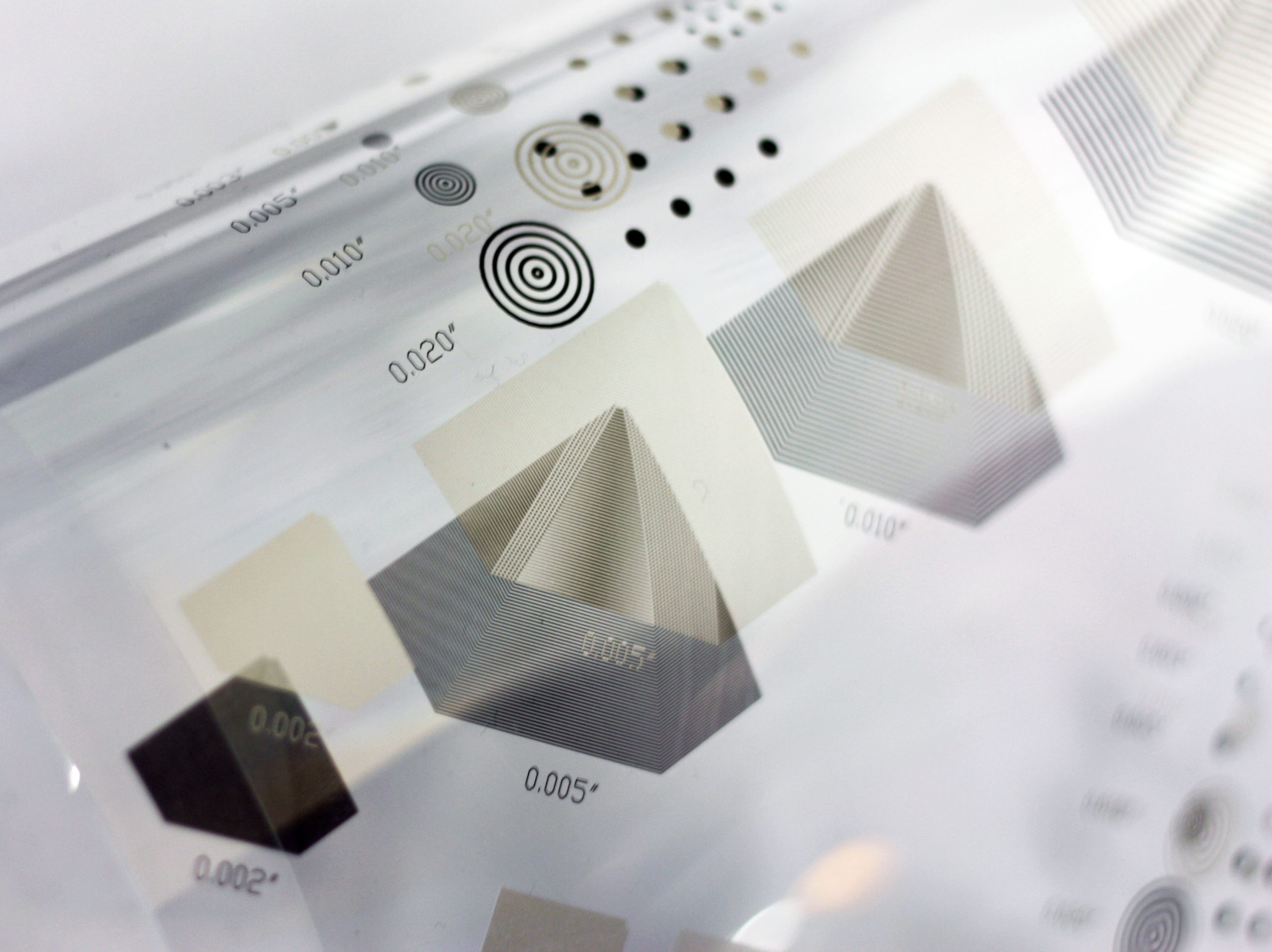
Fine line screen printing leverages the thinness of wire meshes to create conductive lines as narrow as 50µm or even narrower. This method is particularly suitable for applications requiring high-resolution conductive patterns, such as solar cells, touch panels, and low-temperature co-fired ceramic (LTCC) electrodes.
Calendered Wire Mesh: Enhancing Performance
Calendered wire mesh is a process that enhances the performance of screen printing in several ways. By flattening the mesh using the high-pressure rollers, this method stabilizes the mesh structure, leading to improved dimensional accuracy. The flattened knuckles of warp and weft wires result in a thinner paste deposit and smoother surface, contributing to better print resolution.
Hybrid Solutions: Combining Screen Printing and Laser Patterning
Hybrid solutions combine the strengths of screen printing with laser patterning to achieve fine-line printing with extreme dimensional accuracy. This method is particularly valuable for applications like touch screen edge electrodes, where complex patterns demand precise and repeatable results from both the screen and printing machine.
Direct Ultra-fine Line Printing: Pushing the Boundaries
Direct ultra-fine line printing is at the forefront of fine line printing technology, pushing the boundaries of what is possible. This method involves wire meshes with wire diameters as thin as 20µm, high-resolution emulsion, and glass masks, resulting in extremely fine conductive lines. Applications for this technology include TFT backplane metallization, transparent RFID antennas, and printed electronics sensors.
Offset-Based Printing: A Smoother Approach
Offset-based printing offers a smoother approach to fine-line printing by embossing fine grooves into the substrate and then filling them with conductive ink. This method provides precise and smooth conductive lines, and the depth of the grooves can be adjusted to achieve higher conductivity levels without compromising line width. It is particularly well-suited for large-area transparent heating applications.
Pushing the Limits with Fine Line Printing
As technology continues to advance, the methods for fine-line printing are constantly evolving. Advances in screen printing, hybrid solutions, and direct ultra-fine line printing are pushing the limits of what can be achieved in electronics manufacturing. These methods are opening doors to new applications and revolutionizing industries such as solar cells, touch panels, and flexible electronics, and we at e2ip are committed to being at the forefront of these developments.
e2ip – Your Partner in Precision Fine Line Printing Solutions
Fine-line printing is a cornerstone of modern electronics, enabling the creation of smaller, more advanced components. e2ip‘s expertise and dedication to innovation make us a trusted partner for companies seeking to leverage solutions such as fine-line printing, conductive inks for printed electronics, and more. We encourage you to explore the vast potential of fine-line printing– e2ip technologies is here to help you from ideation to fabrication.