Exciting Opportunities for Printed Electronics and Printed Sensors in Future Medical Applications

The printed electronics industry has existed for decades, and today, printed electronics are commonly found in almost every modern device. Their lightweight, compact, and flexible design contributes to their widespread adoption across various industries. Additionally, cost-effective manufacturing techniques have made them ubiquitous to the extent they have become almost invisible and often go unnoticed, yet they continue to play a crucial role in introducing and enabling new functionalities, improving product quality, and enriching user experiences.

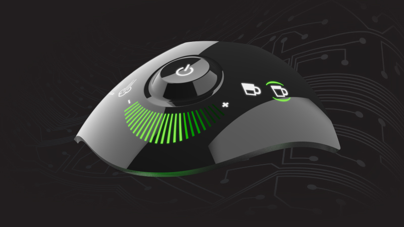
The industry is once again experiencing a resurgence due to recent innovations and material advancements, leading to new and exciting possibilities, while concurrently elevating and improving existing technologies. One notable advancement is Printed Sensors, which represents a natural progression in this field.  Printed sensors seamlessly integrate sensing capabilities directly onto or into electronic devices to detect a wide range of physical and chemical parameters. Their versatility unlocks endless opportunities for innovative solutions in medical, healthcare and fitness applications, offering cost-effective sensor solutions that can be tailored for various use cases.

Biosensors vs Biometric Sensors

In the context of printed sensors used in medical devices and healthcare applications, it is important to understand the fundamental difference between biometric sensors and biosensors. Although both sensors share similarities, their underlying principles and applications are different and distinct.

Biometric Sensors:

Biometric sensors serve the primary purpose of capturing and analyzing unique human and physical characteristics, typically for identification or authentication purpose.  These sensors capture and analyze specific biometric data, such as fingerprints, facial features, iris patterns, or voice patterns, and use this information for user identification or verification. Biometric sensors are commonly used in access control systems, identification processes, and security applications.

Biosensors:

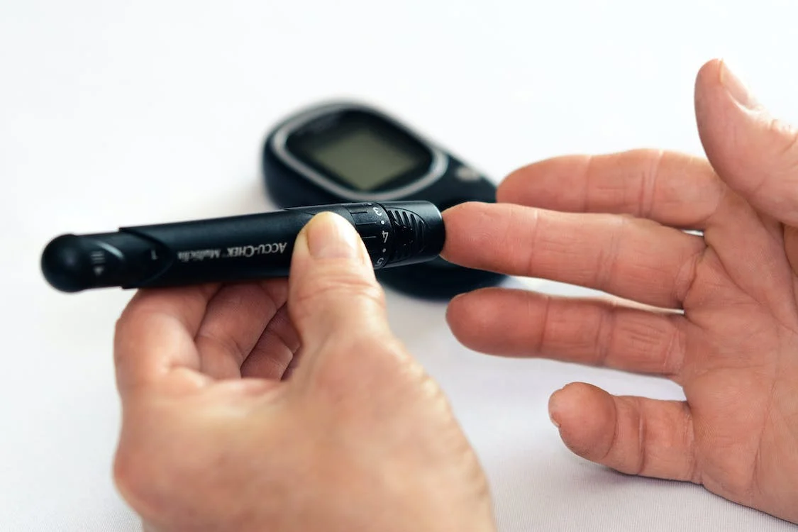
Biosensors are analytic devices that convert a biological or physiological response or marker into an electrical signal.  Biosensors can be external in nature, such as the glucose strip of a glucose monitoring device, or they can be attached or worn on the human body and are commonly integrated into wearable devices for continuous health monitoring and tracking.

Examples include ECG sensors, which measure and monitor a heart’s electrical activity, EEG sensors which monitor brain activity, and biological sensors that are capable of measuring and monitoring biological substances for biomarkers such as glucose, cholesterol, pH levels, proteins, or pathogens.

Although biosensors are typically non-invasive in nature, they can be designed as implantable devices that offer unique advantages for long-term monitoring capabilities, thereby expanding their potential applications in healthcare.

Despite their differences, the terms “biometric sensors” and “biosensors” are often loosely interchanged because they both involve biological signals and measurements.  However, it is important to be precise and contextually aware when using these terms to avoid unnecessary confusion.  For the sake of clarity and consistency in this context, we will use the term ‘biosensor’ to refer to sensors that detect and measure specific biological or physiological parameters for diagnostic and monitoring purposes in healthcare.

Changes in Healthcare and the Medical Industry

A Not-So-Distant Scenario

Imagine this scenario: A man is cycling in the park when his wearable sensor detects early signs of a potential stroke, triggering an instant alert. Simultaneously, the information is sent to both his personal AI provider and his family. The AI promptly analyzes the data and administers life-saving medication through a conductive printed patch, which the man already carries for such emergencies.

At the same time, his family receives the notification and acts promptly to offer support and assistance. They have the option to either call for emergency services or rush to his location to be by his side and provide support and assistance. Alternatively, depending on the severity of the event, the man can opt for a nearby solution by riding just 5 minutes to his local pharmacy to get a refill of the printed patch.

This scenario illustrates the immense potential of cutting-edge technology, including wearable biosensors, AI algorithms, and printed electronics, in transforming healthcare and emergency response. With real-time monitoring, quick analysis, and timely interventions, such innovations are poised to improve outcomes and save lives.

The introduction of telehealth and telemedicine marked the beginning of effective outpatient healthcare solutions, enabling remote consultations & medical services outside the traditional healthcare setting.  Similarly, the introduction of EMR (Electronic Medical Records) revolutionized how medical data is collected, recorded & stored, with significant benefits in downstream studies and analytics to help aid in identifying patterns, trends and correlations in patient data and predicting outcomes.

The healthcare industry continues to change and evolve and is now making a transformative shift towards “Smart” and connected solutions, driven by a growing need for real-time and remote monitoring in outpatient settings. This shift involves the integration and use of cutting-edge technologies such as Artificial Intelligence (AI), virtual assistance, Internet of Things (IoT), NFC, and wireless networking and communications, and printed electronics and sensors. These advancements hold the potential for profound implications in patient care, not only within medical facilities but also in the realm of in-home healthcare.  With mounting strains and challenges on already limited resources, healthcare facilities are actively exploring various options to reduce and mitigate burden and waste, to help optimize healthcare diagnostics and treatment delivery, and to create a more responsive, resilient, and efficient healthcare system that ultimately improves patient treatment and outcomes.

The Potential of Printed Electronics and Printed Sensors

Printed electronics is an innovative and continuously evolving and advancing technology that has revolutionized the design and production of medical devices and sensors. Recent breakthroughs have significantly contributed to the advancement of printed sensors in medical applications:

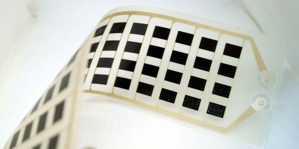
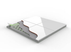
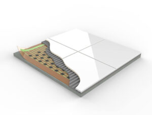
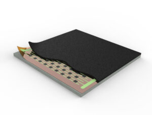
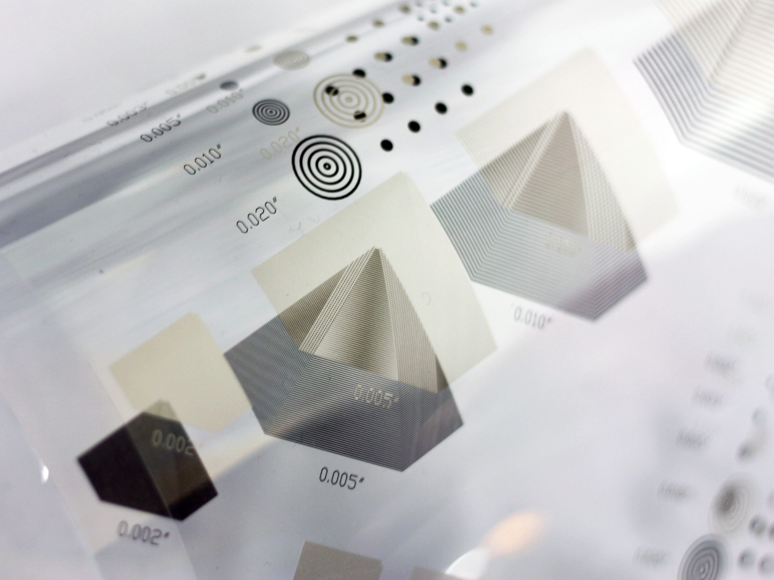
Fine-line Printing:  Advanced printing methods and capabilities can achieve ultra-fine printing resolution has enabled the creation of intricate and highly precise sensor patterns. Fine-line printing techniques can improve the accuracy and sensitivity of sensors, making them more suitable for detecting subtle changes in physiological parameters.

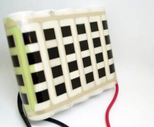
Functional Inks: The development of specialized functional inks has expanded the range of sensing capabilities. For example, conductive inks with enhanced biocompatibility and biodegradability have enabled the integration of sensors directly onto or into the human body without causing adverse reactions.  Molecular inks can be formulated to offer specific properties and functionalities such as improved sensitivity and accuracy, or to react to specific biological substances or biomarkers.

Transparent Inks:  Allows for the creation and printing of near-invisible, discreet wearable devices that can be applied directly to the skin without being visibly intrusive, which patients can wear without feeling sub-conscious.  Additionally, transparent inks are well suited for integration into sensors requiring optically clear or transparent/translucent properties, such as heart rate monitors, oxygen saturation sensors, or imaging sensors.

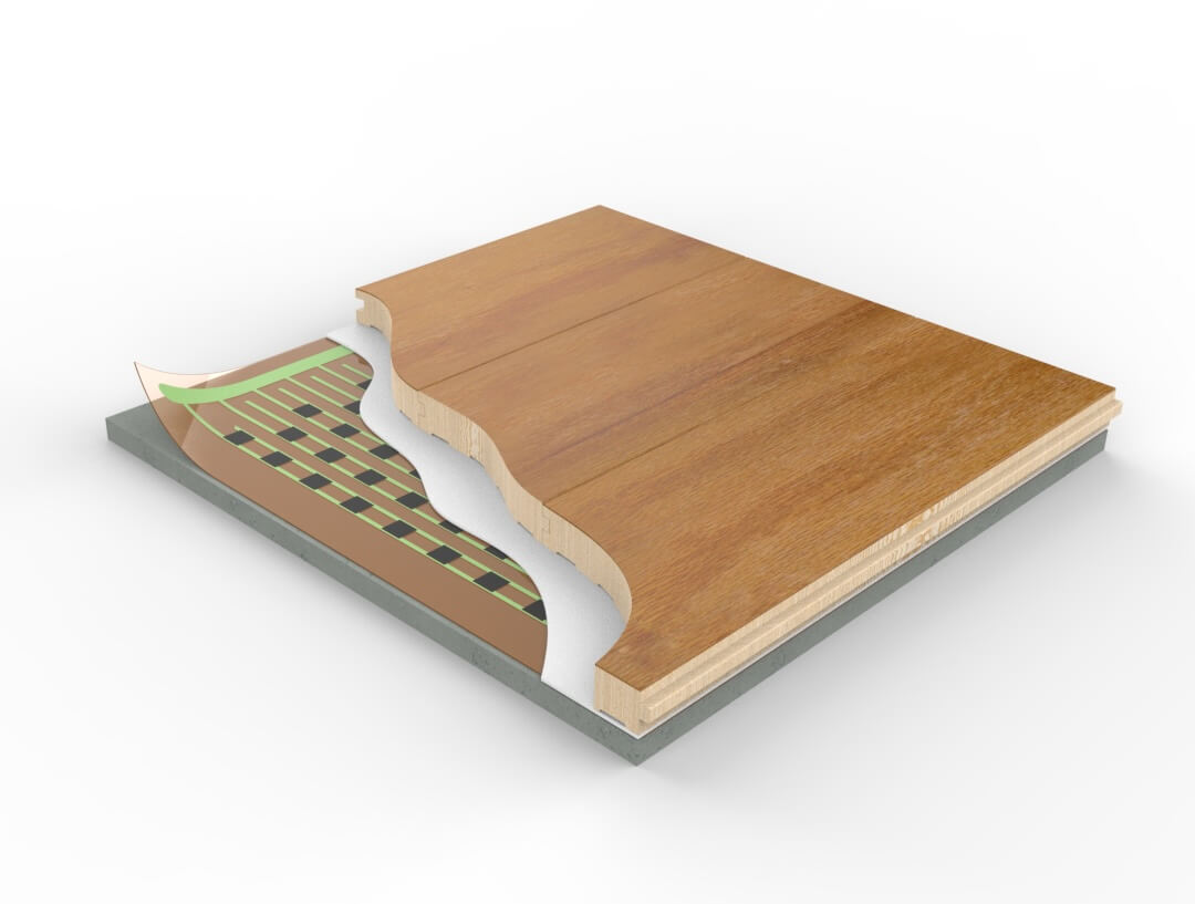
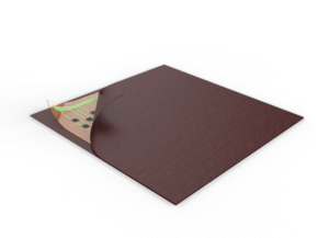
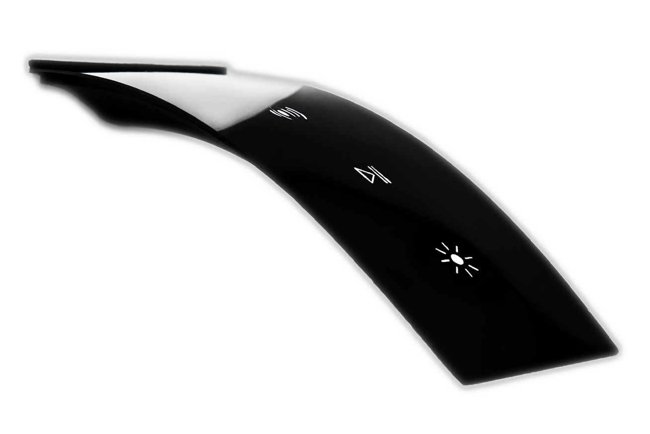
Flexible and Stretchable Substrates:  Printing sensors on flexible and stretchable substrates allows them to conform better to the curved shapes of the human body. This innovation has led to the creation of wearable sensors that are comfortable to wear and unobtrusive.

Multi-Modal Sensing: Advanced printed sensors can now detect multiple parameters simultaneously, offering multi-modal sensing capabilities. For instance, a single sensor may measure both temperature and pressure, providing a comprehensive assessment of a patient’s condition.

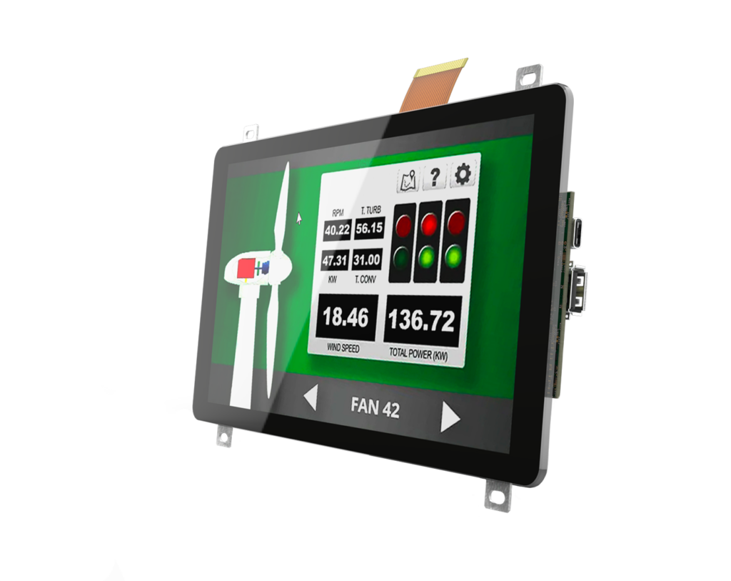
Wireless Communication: Printed sensors with wireless communication capabilities can transmit real-time data to healthcare providers, enabling remote patient monitoring. This breakthrough has enhanced telemedicine applications and improved patient care, especially in remote or home-based healthcare settings.

Hybrid Integration: Printed electronics can now be seamlessly integrated with other components, such as microcontrollers or batteries, enhancing the overall functionality of printed sensors. This integration enables the development of more sophisticated and versatile medical devices.

The continuous advancements and breakthroughs in printed electronics and sensors have significantly enhanced their potential and applications in the medical industry. As a result, there is a growing adoption of printed electronics and sensors in healthcare, benefiting from their versatility and customizable form factors. These advancements offer many advantages, including quicker detection and diagnosis, improved accuracy and reliability of sensor data, enhanced patient comfort and convenience, self-monitoring capabilities, and cost reduction across the healthcare ecosystem.

One area where printed sensors have had a significant impact is in the development of inexpensive, flexible, and wearable technologies. These lightweight devices can be directly applied to the skin or seamlessly integrated into clothing, enabling various medical applications such as therapies, medicine delivery, and continuous monitoring. The ability to print sensors on flexible and stretchable substrates allows them to conform better to the curved shapes and repeated movements of the human body, making them comfortable for long-term wear.

Moreover, printed sensors can be designed for either long-term use or as disposable applications, with the latter being extensively used in healthcare facilities to reduce infection risks and prevent pathogen transmission. The materials used in disposable sensors are non-toxic and easily biodegradable, making them both cost-effective and environmentally sustainable.  Additionally, materials can be enhanced with anti-microbial properties, providing an added layer of protection, and enhancing both patient and caregiver safety.

Sensors play a crucial role in monitoring various physiological parameters like heart rate, temperature, blood pressure, and respiratory rate. Their integration into medical devices and implantable solutions improves patient care, diagnosis, and overall health monitoring in a cost-effective and sustainable manner.

The continuous progress in printed sensor technology is driving a revolution in the medical industry, paving the way for innovative and efficient healthcare solutions. The future holds even more promising innovations that will further transform the medical sector, providing improved healthcare solutions and enhancing patient well-being. Additionally, the convergence of printed electronics and sensors with other state-of-the-art technologies like In-Mold Electronics (IME) will unlock new possibilities and opportunities for growth and advancement in medical devices and healthcare solutions.

Reliable Sensors – Key to Quality Medical Treatment

The design and manufacturing of printed sensors requires multi-disciplinary knowledge and expertise across various disciplines.  Additionally, the design and manufacturing of accurate  and reliable printed sensors relies on several key aspects:

Robust Sensor Design: Creating robust printed sensors requires careful consideration of the unique demands of the intended application. The layout and design of the printed circuit are critical factors influencing the sensor’s accuracy. Key elements like trace width, spacing, pattern and alignment directly impact the electrical conductivity, sensitivity, and signal integrity of the sensor. Additionally, the design must account for the sensor’s long-term reliability and durability, particularly when deployed in real-world medical scenarios, where exposure to diverse environmental conditions or biological fluids is likely. By paying close attention to these design aspects, printed sensors can offer optimal performance and longevity in their intended applications.

Sensor Type and Technology: Selecting and designing the appropriate sensor type and technology is crucial. Printed sensors can come in various forms, including electrochemical sensors, biosensors, strain sensors, and temperature sensors, among others. The choice depends on the targeted application and the parameters to be measured. Additionally, it might be advantageous to design the sensor as multi-model, capable of measuring and monitoring multiple parameters simultaneously.

Material Selection: Choosing the right materials, including conductive inks, substrates, and functional coatings, is essential for sensor performance. The materials should be biocompatible, stable, and capable of maintaining consistent electrical properties over the intended life or usage of the sensor.

Power Consumption: For wearable sensors or remote monitoring devices, low power consumption is critical to prolong battery life and enable extended use without the need for excessively frequent or extended recharging times.

Industry and regulatory Standards :In the design and manufacturing of sensors, it is essential to adhere to all relevant industry and regulatory standards and guidelines. Doing so ensures that the products meet the necessary safety, performance, and quality requirements. By following these standards, manufacturers can produce sensors that are reliable, effective, and compliant with established norms, fostering confidence in their performance and usability.

Algorithms and signal processing: Algorithms and signal processing are essential components in the design of printed sensors. They play a critical role in converting the raw analog signals generated by the sensor into digital information that can be effectively analyzed and utilized for various applications. Raw data often contains unwanted noise and interference, which can negatively impact the accuracy and reliability of the sensor’s measurements. Algorithms are employed to enhance the signal-to-noise ratio, resulting in more precise and dependable readings. By effectively processing the sensor’s signals, algorithms ensure that the data collected is of high quality and can be effectively used for real-world applications.

In the medical industry, additive manufacturing and established printed electronics techniques are used to produce sensors for a diverse range of healthcare applications, resulting in cost-effective sensors and medical device production.  As new technologies and advancements are embraced and integrated, the potential for printed electronics in medical applications continues to evolve and grow.

e2ip’s Role in Medical Printed Electronics Innovation 

Choosing a reputable manufacturer with practical experience, extensive technical expertise, advanced processing capabilities, and a proven track record and reputation of consistently delivering high-quality printed electronics and sensors is crucial.

At e2ip Technologies, we have the qualifications and expertise required to meet your specific membrane switch requirements. With our longstanding presence as an industry leader and a proven history of innovation, we invite you to get in touch with us today and provide details about your project. We are prepared to address any inquiries you may have, and our dedicated team of experts is committed to helping you find the ideal solution that perfectly aligns with your unique needs.

To learn more about how e2ip can support your need, product, or project in any industry, contact us or call us in the Montreal area at (514) 631-6662 or internationally, at 1-866-631-6662.  

Revolutionizing 5G Network Deployment with 5G Smart Surfaces

The advent of 5G technology promises to bring about a transformative era of unprecedented connectivity and communication. However, the successful deployment and optimization of 5G networks present a series of challenges, including signal propagation, interference, and coverage. To address these hurdles, engineers and researchers are turning to a cutting-edge solution known as Engineered Electromagnetic Surfaces (EES) or 5G Smart Surfaces. In this blog, we will explore how 5G Smart Surfaces can significantly impact 5G network deployment, revolutionizing the way we experience connectivity.

Understanding 5G Smart Surfaces

5G Smart Surfaces, often referred to as electromagnetic metamaterials or metasurfaces, are passive surfaces designed to manipulate and control electromagnetic waves in novel ways. Unlike conventional materials, 5G Smart Surfaces artificially enhance wireless coverage at microwave and millimeter-wave frequencies via printed conductive patterns on substrates such as plastic, wallpaper or glass.

5g-smart-surfaces-e2ip technologies

Enhanced Signal Propagation and Range

One of the critical challenges faced during 5G deployment is ensuring reliable signal propagation and sufficient coverage, especially in urban areas with high-rise buildings and dense infrastructure. 5G Smart Surfaces can play a vital role in overcoming these obstacles. By strategically placing 5G Smart Surfaces near 5G antennas, it is possible to manipulate and redirect the signal propagation in specific directions, thus optimizing the propagation path and extending the range of the wireless signal. This capability translates into better coverage and reduced signal loss, enabling a seamless 5G experience for users across a broader area.

Minimizing Interference and Enhancing Capacity

In densely populated urban environments, interference between neighboring 5G cells can significantly impact network coverage. 5G Smart Surfaces offer a unique advantage in this regard. By tailoring the electromagnetic properties of these surfaces, engineers can create “stealth” materials that can either absorb, redirect, or diffuse the signal in a desired direction effectively either minimizing the adverse effects of signal overlap or enhancing the overall network capacity. This opens new possibilities for densely packed 5G cells, enabling network providers to optimize resource allocation and deliver improved data speeds and user experiences.

Overcoming Obstacles and Line-of-Sight Limitations

Outdoor Demo Video

Indoor Demo Video

5G’s high-frequency millimeter waves have the potential to deliver astounding speeds and low latency, but they are susceptible to obstacles like buildings and foliage. 5G Smart Surfaces can be designed to work as “smart mirrors,” reflecting and bending millimeter waves around obstacles, effectively establishing non-line-of-sight connections. This capability expands the possibilities of 5G network deployment, as providers can establish connectivity in challenging environments where direct line-of-sight transmission may not be feasible.

Energy Efficiency and Reduced Environmental Impact

As the world increasingly focuses on sustainability, energy efficiency in communication technologies becomes crucial. 5G Smart Surfaces can aid in reducing the power consumption of 5G networks. By controlling the electromagnetic wavefronts passively and with precision, these engineered surfaces can optimize signal transmission paths, reducing the need for high-power transmissions. The result is a more energy-efficient network that not only reduces operational costs but also minimizes the environmental impact associated with 5G deployment.

Future-Proofing the Network

5G is just the beginning of our journey towards a hyper-connected world. As we set our sights on future generations of wireless technology, the flexibility and adaptability of 5G Smart Surfaces become invaluable. These engineered surfaces can be designed and configured to support evolving communication standards, ensuring that the network infrastructure remains relevant and capable of seamlessly integrating with upcoming technologies.

5G Smart Surfaces are set to revolutionize the way we deploy and experience 5G networks. From extending coverage and enhancing capacity to overcoming line-of-sight limitations and reducing interference, 5G Smart Surfaces offer a host of advantages that pave the way for a more connected and efficient future. As researchers and engineers continue to push the boundaries of electromagnetic metamaterials, we can expect even more innovative solutions to address the challenges of 5G deployment and future wireless communication technologies. With 5G Smart Surfaces at the forefront of this technological revolution, the future of 5G networks appears brighter than ever before.

With our innovative technology and commitment to advancing the field of smart surfaces, we at E2IP TECHNOLOGIES, seek to apply our many years of experience in the field of electronics, creating technologies like smart touch surfaces and more, to help push this technological revolution forward. Contact us today for more details about our 5g smart surfaces.

In-Mold Electronics (IME): How In-Mold Decorating (IMD) and In-Mold Labeling (IML) are Changing the Game for Designers

In-Mold Electronics (IME), or Smart Structural Surfaces™, promise to be a game-changing technology that will significantly improve process optimization. 

IME provides for a streamlined production process over traditional electronic assembly. Simply put, IME is a three-step process which includes the printing of electronic circuits and graphics, followed by the forming and molding. However, In-Mold Electronics is often confused with related processes, namely In-Mold decorating (IMD) and In-Mold Labels (IML).

What is the Difference Between IML and IMD?

IME’s roots are tied to both IMD and to a lesser degree IML. IME takes the process of printing, forming, and molding to a new level of complexity. Both IMD and IML offer a streamlined process utilizing printing, forming and molding. All three offer an enhancement in the production of parts with complex 3D geometries. 

An In-Mold Decorating or In-Mold labeling process only offers a decorative function. Typical examples of IMD include molded plastic parts, such as mobile phone covers. In-Mold labels can be found in a broad variety of plastic containers and consumer packages, such as for ice cream tubs, shampoo bottles, and many more. 

                    Ice creams tubs IML

In-Mold Electronics specifically describes a more complex process which, like IMD and IML, begins with fundamentally the same three primary processes of printing forming and molding. However, IME is dramatically different in that it marries electronic functionality to the decorative process making the part a functional Human Machine Interface (HMI) for industrial or consumer applications. These parts are referred to at E2IP as Smart Structural Surfaces™. 

Smart Structural Surfaces™: A Step Forward for IME

The IME process begins by printing stretchable conductive inks onto a film to create fully functional electronic circuits. A graphic overlay is printed onto the second film. These graphics align with the electronic circuitry and can include icons for intuitive user interaction as well as to serve the aesthetic design. The films are then thermoformed into the desired 3D shape. Electronic components can be added to the circuits before or after thermoforming. The part can include lights, sound and haptic feedback. The graphic layer and the circuit layer are placed together in the mold cavity of an injection mold. The injection molding embeds all the components creating a single, rigid molded plastic part.

Smart Structural Surfaces™ offer a range of benefits over traditional HMI components, including increased durability, reduced manufacturing costs, and improved design flexibility. By eliminating the need for additional assembly and reducing the number of components needed, Smart Structural Surfaces can significantly reduce production costs and waste.


Avatar A*


Avatar B*

Avatar C*

Printed circuit with sensors Printed graphic with icons and design theme Exploded view of the Smart Structural Surface™

*Avatar represents a complex design and is an example of IME potential. 

The Advantages of Smart Structural Surfaces™ 

  • Reduced production time
  • Fewer components
  • The elimination of mechanical parts
  • Thinner, lighter parts
  • Lower cost 
  • Improved reliability

Unlocking New Design Possibilities

The manufacturing industry is constantly evolving. All three In-Mold Decorating, In-Mold Labeling & In-Mold Electronics are serving as game changers by enabling graphic and industrial designers the freedom to execute messages and concepts on surfaces and shapes they could not have dreamed of before. 

Our In-mold electronics process takes IMD and IML to the next level by integrating fully functional electronic components into the molded plastic part. This means that electronic circuits Like capacitive touch switches , lights, sound, and haptic feedback can all be embedded directly into the plastic part, eliminating the need for additional assembly and reducing production costs.

By leveraging our cutting-edge process, companies can reduce their production costs and waste while increasing their manufacturing efficiency. The process also enables designers to execute their messages and concepts on surfaces and shapes they could not have dreamed of before, providing new possibilities for product design and development. It allows for high-quality, durable graphics to be embedded directly into plastic parts, while also enabling the integration of fully functional electronic components. These processes not only reduce costs and waste but also provide designers with the creative freedom to execute their ideas on surfaces and shapes they previously thought impossible.

Contact us to learn more about In-Mold Electronics & Smart Structural Surfaces™. 

Developing Sustainable Electronics

Between the materials used to produce electronics and electronic waste, the electronics industry is turning its attention to issues of sustainability. Global e-waste is expected to double by 2050, so sustainability efforts are clicking into gear not a moment too soon.

The electronics industry can respond to the call for sustainable solutions by creating consumer electronics in new ways, including bio-based materials and printed electronics. Environmentally sound design choices can also play a role in improving the industry’s sustainability.

On their end, consumers are also demanding greater attention to environmental sustainability. They’re paying attention to disposal of hazardous waste and opting for refurbished electronics, among other choices.

As electronics companies create sustainable electronics, use recycled plastic and other materials for packaging, and recycle electronics in a responsible manner, they can join with consumers to mitigate climate change and other negative environmental impact.

Why Is Sustainability Important for the Electronics Industry?

Sustainable choices are important for the industry because they conserve precious natural resources and protect the environment.

Manufacturers can use environmentally friendly materials that can be recycled easily in order to reduce their impact on the environment. By doing so, they can help to remove these materials from the waste stream and prevent them from contributing to pollution and other environmental problems. Additionally, by paying attention to the carbon footprint of their supply chain, manufacturers can reduce their overall impact on the environment by minimizing the amount of greenhouse gases that are emitted during the production and transportation of their products. By taking these steps,

manufacturers can send a message to consumers that they are committed to ethical, sustainable, and carbon neutral practices. This can help to attract consumers who are increasingly seeking out products that align with their values and support a more sustainable future.

Blog-Header-Sustainable-Electronics

How Can Electronics Be More Sustainable?

To measure the environmental impact of electronics, you have to look at several factors, including the design process, the manufacturing production cycle, the raw materials, and the recycling of materials after use. Each electronics product has a different life cycle, so environmental impacts can vary from one product to the next.

Take a look at some of the options and novel solutions available for lightening the environmental load of electronics products.

Printed Electronics

Printing electronics drastically limits the amount of fossil materials used, as thin electronics and wearable devices are printed on various substrates using either traditional or novel printing equipment. In addition, energy consumption is significantly reduced with printed electronic components. Printed electronics are useful for flexible displays, sensors and various human-machine interfaces.

Use of Hazardous Chemicals

Many electronics products use heavy metals and toxic chemicals that are harmful to human health. These include lead, mercury, cadmium and various flame retardants. Electronics manufacturers can help manage these hazardous materials through eliminating PVC (polyvinyl chloride) from their power supply and cabling products and by choosing materials that don’t need flame retardants.

Energy Efficiency

Manufacturers can look for ways to save energy during the production of devices. They can also design products that are energy-efficient by tapping into ENERGY STAR features and adding low-power standby modes. Self-powered devices that offer energy harvesting from body motions lower energy demand, and use of supercapacitors reduces the need for lithium batteries.

Product Design and Materials Management

Products that require fewer resources and materials tend to generate less electronic waste at their end of life. It may be possible for some manufacturers to switch to sustainable materials such as vegetable-based plastics, recycled plastic, aluminum or recycled glass to minimize e waste as well. The same can be done with product packaging to lower each product’s overall carbon footprint. In addition, designing products that need reusable batteries rather than single-use batteries helps.

Sustainability for Consumers: How to Buy Electronics Ethically

Consumers play an important role in developing sustainable electronics. The more they demand eco-friendly electronics and a sustainable future, the more the technology industry responds.

They can pay attention to the supply chains used by their favorite brands. In the past, buyers had no way to know when a company was using child labor in developing countries, for example, in an effort to gain a competitive edge. Now, organizations such as Amnesty International have provided evidence showing that electronics companies are often responsible for human rights abuses.

When consumers put pressure on shareholders and companies, demanding ethical supply chains, living wages for workers, use of recycled materials, lowered carbon emissions, and other sustainable production choices, the industry is bound to take notice and make smart choices.

Sustainability and Corporate Responsibility

Electronics manufacturers play a key role in encouraging environmentally friendly electronics by using sustainable materials and manufacturing processes, and by designing products that are energy efficient and have a long lifespan.

Governments can also play a role by implementing regulations and incentives that promote the use of sustainable electronics, and by supporting research and development of environmentally friendly technologies.

Product designers can help by creating electronics that are easy to repair and upgrade, which can extend their lifespan and reduce the need for replacement. Consumers can support environmentally friendly electronics by choosing products that are made from sustainable materials and have a low impact on the environment, and by disposing of their electronics responsibly at the end of their lifespan.

e2ip_well-directed-impact-768x575

By working together, electronics manufacturers, governments, product designers, and consumers can all help to create a more sustainable future for electronics.

At e2ip Technologies, we go beyond the minimum of meeting environmental compliance regulations by producing sustainable electronics that respect the environment, focusing on energy efficiency through all aspects of our process, promoting recycling and reuse of electronic products and packaging, and far more. We are fully committed to doing everything we can to promote environmental sustainability, minimize pollution, and be part of the solution. If you would like to learn more about sustainable electronics, contact us today.

Fine Line Screen Printing: Challenges and Possibilities for Printed Electronics

Screen printing is a technique that has been used for centuries to create beautifully printed image artwork on a wide variety of surfaces. Today, screen printing is used in more applications than ever, ranging from creating artwork and signage to advanced printed electronics. Thanks to its versatility and durability, screen printing is a technique that will continue to have a lot to offer for a wide range of evolving uses.

This post will delve into some of the challenges and opportunities for this technology to play an important role in the future of printed electronics and human-machine interfaces.

An Overview of The Screen Printing Process

At its core, screen printing involves creating a stencil of the desired image on a screen, and then using that screen to transfer the image onto a substrate. In this additive process, stencils are used to transfer inks or other materials onto the substrate. The “stencil” is essentially a screen that allows the ink to pass through onto the substrate below. Screen printing is a versatile process that can be used for a wide range of substrates, including flexible materials.

Although screen printing is most commonly associated with printing photographic images, a similar process is used to create printed electronics. In this type of manufacturing, advanced mesh screens and conductive inks are used to create functional electronics on a wide range of flexible substrates.

One advantage of screen printing is that it can be used to print very thin and precise patterns on a diverse range of substrates. Additionally, screen printing can be used to create multilayer prints with high accuracy and repeatability. This makes screen printing an excellent choice for printed electronics applications.

screen-printing-finale-1024x522

Printed Electronics Advantages

Screen-printed electronic components offer several advantages over traditional wires and circuitry. Wear and tear from use, combined with the potential for oxidation, tends to limit the lifespan of electronic components, however, printed electronics do not share these limitations. Printed circuit assemblies are lightweight, sturdy, and long-lasting.

Printed electronics are typically thinner and more flexible than conventional electronic components, which can improve the ergonomics of an assembly. Also, printed electronics are printed directly onto a substrate, which eliminates the need for separate printed circuit boards or other wiring harnesses, which reduces the overall size and weight of an assembly, as well as the number of potential failure points. Most importantly, printed electronics can be custom-tailored to specific applications, which allows for far greater design freedom and flexibility. For these reasons and others, printed electronics will continue to significantly improve the capabilities, performance and reliability of human-machine interface assemblies.

Printed Electronics Applications

  • Printed heaters
printed-heater-e1504806340248-300x234
  • 5G Smart Surfaces
e2ip_5G-rebound-thumbnail

Overcoming Technical Challenges

For many electronic components, screen printing remains a highly cost-effective production method, however, there remains the technical hurdle of achieving sufficient resolution for the next generation of printed electronics. Challenges include mesh clogging, finding the right inks, and repeatability, particularly when printing at less than 40 microns. There are advancements that are continually being made in the field of screen printing and this threshold is likely to continue to shrink in the years to come.

e2ip technologies is an industry leader in this regard, thanks to a fine line printing method and proprietary conductive inks, that allow for lines with sub-micron trace thicknesses. In order to screen print image resolution with such fine lines, while minimizing interference or misalignments, it requires the use of wire meshes with the thinnest possible diameter wire, as well as advanced electrical conductive inks.

The Advantages of Advanced Conductive Inks

Meeting the demands of current and next-generation printed electronics requires constant innovation, specifically to resolve the limitations of traditional flake inks. Through the creation of advanced conductive inks, e2ip technologies is once again at the forefront of research, development and implementation of novel solutions to longstanding obstacles in the screen printing process for electronic applications.

Based on ionic molecules derived through a reduction process, e2ip’s molecular ink (MINK), developed in collaboration with the National Research Council of Canada (NRC), solves several technical challenges at once. It enables a simplified, affordable fabrication process, greater design freedom and a reduced ecological footprint, which makes them an appealing option for many applications. MINK sets itself apart from other conductive inks thanks to its high conductivity, elongation, formability, and flexibility.

The Potential for Advanced Fine Line Printing & Conductive Inks

The computer you are using to read this was, at one point, the size of a room. Now, it can fit in your pocket. This incredible shrinking trend is occurring across a variety of industries as the world demands more functionality in smaller and smaller devices, printed electronics is one area where this trend is especially apparent.

As the demand for faster, thinner, lighter and more flexible electronics increases, screen-printed electronics will play a more important role in a wide range of industries, such as aerospace, medical, defense and automotive.

Screen printed solutions from e2ip technologies use various conductive inks, including MINK, and are compatible with a wide variety of lightweight, flexible substrates that can be used to create energy-efficient and cost-effective printed electronics, membrane switches, 5G Smart Surfaces and more.

If you would like to learn more about these technologies and their potential for the creation of innovative products, contact e2ip technologies today.

Advanced Human Machine Interfaces: Elevating the Airline Passenger Experience

The human-machine interfaces (HMIs) in an aircraft do more than relay information. They connect passengers to the crew and the crew to the aircraft. The right design and implementation of HMIs create the foundation for an optimal experience.

The passenger experience is one of the most important factors in designing an onboard human-machine interface, but HMIs go beyond allowing passengers to control their seats, adjust their lighting, and select their in-flight entertainment. HMIs are also essential for pilots and crew to perform their duties. 

The design and features of HMIs, such as backlighting, the type of feedback provided, and the feel of materials, make critical contributions to the final design. The challenge for aerospace manufacturers is twofold: to incorporate HMIs in ways that are intuitive, and to do so in ways that make them easy to integrate into the overall design concept while respecting engineering constraints and aesthetic concerns.

The HMI Challenge: Meeting Aerospace Industry Standards While Improving the User Experience

It is also important to understand human-machine interface requirements in the context of time and space – it’s not just about designing human-machine interfaces for today’s passengers, but designing interfaces that will meet the needs and demands of the future of air travel.

In commercial airplane cabins, the limitations on available space are baked-in design constraints, which greatly limited HMI options in the past. Add to those the need to ensure that HMIs meet industry and manufacturer standards, including meeting rigorous quality and reliability protocols while providing the required protection against shock and vibration, and the result is the previous generation of HMIs, full of limitations and shortcomings.

Thankfully, advancements made in materials and design now permit interfaces that can make use of these hitherto underused spaces to integrate the next generation of aerospace industry compliant HMIs, ones that will continue to optimize the passenger experience.

Using Technical Innovation and Design Expertise to Improve the User Experience

The most successful HMI designs integrate ergonomics, technical specifications, and engineering constraints in subtle ways to create interfaces that are not only aesthetically pleasing but also maximize ease of use and versatility.

In modern aircraft cabins, HMIs have an important role to play in passenger control units and seat controls, in-flight entertainment controls, galley controls, signage and indicators, lighting, as well as the abundant possibilities for customized touch screen solutions to HMI challenges.

Custom HMIs from E2IP TECHNOLOGIES

Here are just a few examples of how our aerospace products have made the lives of airline passengers easier:

Passenger Control Units (PCU) & Seat Controls

Airplane seats are fundamental to the comfort and overall enjoyment of passengers during their travel experience. As such, designers and engineers pay special attention to the desires of passengers in this area, creating ergonomic, intuitive and customizable PCUs and seat controls.

These robust and reliable products can be tailored to complement our customer’s interior designs with optically balanced and uniform backlighting in various colors, patterns, textures, and icons.

Our mechanical PCUs feature tactile feedback based on micro-switches or metal domes, these products can have a front panel with printed graphics or a silicone membrane with plastic or metal keys. Capacitive PCUs are available with rigid or flexible capacitive sensors that can also deliver tactile feedback, uniform backlighting, and excellent surface scratch resistance.

In-Flight Entertainment (IFE) Controls

To help passengers to enjoy an optimal travel experience, e2ip technologies works closely with major industry players by offering them innovative interfaces such as IFE remotes, USB chargers, touch screens, and others that can be easily integrated into the in-flight entertainment system.

These ergonomic and intuitive products, housed in injection-molded plastic, offer optically balanced backlighting and the choice between projected capacitive or resistive touch screens as well as numerous switch and force options. IFE controls can be tailored to complement cabin interior designs through numerous options for colors, patterns, textures, and icons.

Galley Controls

Efficient and intuitive equipment helps crew members provide airline passengers top-quality service, so it’s important to have controls for cabin and galley equipment that are highly reliable and user-friendly.

Through the use of graphical user interfaces, LCD screen, EMI/ESD shieldings, numerous switch options, projected capacitive or resistive touch screens as well as ample colour, pattern, texture, and icon options, galley controls can be custom-tailored to suit virtually any need.

Lighting Solutions

Designed to elevate the cabin interior experience, lighting solutions can be tailored to suit customer branding and designs through customizable textures, finishes, patterns and colors for reading lights, feature lights, ambient lighting, and mood lighting.

With passenger wellbeing at the heart of design considerations, customized lighting solutions create a sense of home and harmony that helps passengers feel at ease.

Signs and Indicators

Well-designed signs and indicators contribute to a positive travel experience by providing passengers with fluid and seamless access to essential information.

Signs and indicators that address the gamut of interior cabin and passenger needs through customizable graphics and various backlighting options in aircraft-rated assemblies can be designed and produced with different colors, textures, and patterns to suit specific needs and contribute to holistic cabin interior designs.

E2IP TECHNOLOGIES Customized Solutions for Cabin Interior Design

At e2ip technologies, safety, quality and reliability are paramount concerns at every stage of product development. This is true whether we’re drafting the initial design, overcoming engineering challenges, or engaging in the final steps in the manufacturing process.

Having achieved top-level certification standards, including AS9100C, RTCA/DO-160, RTCA/DO-178 and FAR 25.853, as well as various manufacturer’s internal standards, such as Boeing and Airbus, our cabin interior products meet the highest levels of compliance across the aerospace industry.


e₂ip technologies received the highly coveted 2020/2021 Crystal Cabin Award for In-Mold Electronics (IME).

By advancing the materials and processes used in IME, e₂ip has unlocked greater design freedom in the creation of elegant, user-friendly surfaces for the cabin space. Through a design that integrates electronics within the molds of controllers, simple hand gestures enable a variety of controls that allow passengers ultimate control over their surroundings.

We create leading-edge product solutions that meet industry standards and exceed customer expectations.

If you want to learn more about our customized solutions, contact us and a member of our team will contact you shortly.

Everything You Need To Know About Membrane Switches

What are Membrane Switches?

A membrane switch is a user interface device that is made up of several layers and used as a switch to turn a device on or off. Unlike mechanical switches, which are generally constructed with copper and plastics, membrane switches are printed circuits on film.


How do Membrane Switches Work?

The design behind most membrane switches is simple: when an operator presses a button, a contact is made activating the circuit. When the operator releases the button the contact ends deactivating the circuit.


How are Membrane Switches Made?

The design and manufacturing process behind membrane switches is one e2ip technologies  handles with much care and creativity. Membrane switches are made by printing a carbon or silver ink onto various substrates. A customized graphic overlay is then applied to the film. At e2ip technologies , we offer a wide range of graphic layer material, including polyester, antimicrobial polyester, polycarbonate, blends, and silicone. These pliable, durable materials are where “membrane” switches get their name.

Where are Membrane Switches Used?

Membrane switches are used in a number of applications, including in medical, aerospace, defense, industrial, and transport industries. They are often used for keypads, control panels in aircrafts, touch screen phones, and kidney dialysis machines—just to name a few.

Membrane switches are revered for their durability and flexibility, especially in high or low-temperature environments. They are also known for their reliability and high conductivity.

Types of Membrane Switches

There are two main types of membrane switches, each performing different functions on the circuit board

Tactile. Tactile switches are designed to provide a response when pressed by an actuator or finger. An overlay over the switch has symbols or letters used to designate the function of each switch. Generally, these switches are designed using metal domes. When pressed, the metal dome pushes against a conductive footprint, causing an action to happen.

Non-tactile. This type of switch operates with the same concept as a tactile switch but does not elicit a tactile response. With the bottom of the overlay connecting to a conductive pad, non-tactile switches are self-contained units.

At e2ip technologies, we provide a variety of membrane switches for applications in the medical, aerospace, defense, industrial, and transport industries. Our engineering and design teams are committed to providing you with a durable, reliable, and eco-friendly product, guaranteed to improve efficiency within your business. Contact us today for more information about our products.

Achieve Your Design Goals with Novel Backlighting Solutions

As the demand for enriched user experiences and sleeker technology shows no signs of abating, engineering and design teams, across a range of industries, are requiring thinner and more advanced lighting solutions to meet their design needs.

Although existing LED light products are often used, today’s design requirements require backlighting solutions that offer greater design possibilities. The result is that companies are always on the lookout for new backlighting solutions that can provide their products with a competitive edge.

From reigning in the cost of development to permitting new design possibilities and other benefits, Lumifilm® technology has set itself apart from traditional backlighting solutions to usher in a new era of design freedom. Whether the application relates to human machine interfaces, membrane switches, retail displays, decoration, signage, smart-touch surfaces or other electromechanical systems, Lumifilm® ensures even illumination through uniform backlighting that avoids hot spots and shadowed areas.

What is Lumifilm®?

Based on the principle of light guide film, this technology enables the creation of ultra-thin backlighting systems. Light is injected inside a thin film by a light-emitting diode (LED) source which is attached to the edge of the film.

The surface of the film contains printed dot patterns, which are obtained through a screen printing process. When the light diffuses across the surface and hits the printed dots pattern, it creates an illumination effect optimized in a way that ensures a uniform light output. This helps the light sheet avoid problems, such as hot spots and shadowed areas.

What Sets Lumifilm® Apart From Other Light Guide Films?

Unlike the traditional light guide technology that is often used in combination with translucent material, Lumifilm® overcomes the usual challenges of hot spots, light leaks and shadows through a unique, proprietary solution.

In Lumifilm® applications, light is injected by a LED source inside a thin film and is then conducted via Total Internal Reflection (TIR) and extracted locally with printed dots. What sets Lumifilm® apart is the use of e2ip’s proprietary algorithm that has been specifically created for light optimization. n. In addition, e2ip’s design of the dot pattern provides bright and consistent light output.

Lumifilm® is an innovative material that takes LED lighting and design to the next level, and it can be used in any number of applications or applied to custom shapes. Specifically engineered to be integrated into the thinnest application, Lumifilm® offers greater design freedom and lighting solution possibilities than other options on the market, and works well even when the space between components may be highly limited.

What’s best, non-recurring engineering and production costs are remarkably low when using this kind of light source, which eliminates the need to invest in hard tools, such as molds.​ This kind of next-generation printed LED backlighting is flexible, lightweight, and can satisfy all design needs.

Where can Lumifilm® be used?

Lumifilm® technology permits a wide variety of printed backlighting solutions for applications across a diverse range of sectors. Because this technology can be applied to virtually any backlight solution, Lumifilm® can help create new, improved products for the industries as diverse as aerospace, medical technology, telecommunications, defense and transportation, amongst others.

The LEDs are available in a variety of colors and the backlit surface can be customized into any desirable shape, backlighting anything from molded plastics to translucent materials.

Backlighting Solutions for Diverse Design Needs

As a backlighting source, Lumifilm® is a thin, uniform, versatile and customizable light guide film that is suitable for both indoor and outdoor applications.

If you want to learn more about how Lumifilm® technology, in conjunction with design support from ideation to fabrication, can open up a new world of design possibilities contact e2ip Technologies to speak with a specialist.

Embedded Control, Communications and Human Machine Interface Systems

From medical devices to factory automation, there are many embedded systems all around us that have changed how we interact with the world. Advanced embedded control, communications and human machine interface (HMI) systems are responsible for delivering responsive and elegant user experiences across a wide range of industries.

In this blog post, we will explore embedded systems in modern technology and the features and functionality required of touchscreen HMI modules to create the next generation of devices, with a look towards the design and engineering challenges that have held back many industry stakeholders.

What are Embedded Systems?

Embedded systems perform specific tasks with larger machines and devices. There are many types of embedded systems, and they can be found everywhere from industrial machines to  medical equipment to aerospace components.

Industrial embedded systems often have an embedded operating system and embedded software to perform specific monitoring and control functions. Similarly, modern medical equipment contains a wide variety of embedded systems for sensors and control mechanisms.

A basic embedded system is a computing system with its own hardware and software that can interact with various input and output devices. Their hardware and software complexities can vary significantly from application to application, ranging from having no user interface (UI) – for example, on devices designed to perform a single task within a mobile embedded system – to complex graphical user interfaces, such as the smart surfaces found in modern aircraft interior controls.

Embedded System Applications

Embedded systems are required in a wide range of industries, including the food & beverage, energy, medical, manufacturing, instrumentation and white goods sectors. Each of these industries has its own unique needs, but all of them require embedded systems that are reliable, efficient and easy to use.

The food & beverage industry requires embedded systems that can withstand harsh environments and provide accurate measurements. Embedded systems in the energy sector must be able to handle large amounts of data and be highly energy efficient. Medical embedded systems need to be small, lightweight and easy to sterilize. And manufacturing embedded systems must be rugged and able to withstand the rigors of the production line.

No matter the industry, embedded systems must be designed with the user, as much as the application, in mind. The best embedded systems are those that are reliable, easy to use and provide a great user experience.

Embedded Systems in Healthcare

Healthcare devices and equipment, such as diagnostic equipment and imaging systems, rely on embedded control systems. Examples of HMIs and embedded systems working in conjunction include digital flow sensors, magnetic resonance imaging machines, patient monitoring systems, and more medical technology.

Furthermore, the growth of the Internet of Things (IoT) presents new opportunities for embedded operating systems in healthcare. For example, future wearables with real-time operating system capabilities may track health data, such as vital signs, and transmit it to healthcare service providers for instantaneous monitoring and diagnosis.

Embedded Systems & Consumer Product Innovation

The world of consumer products has always looked for ways to deliver increased functionality, however, adapting HMI modules to allow for the integration of more advanced assemblies to industry needs and demands has proven to be quite challenging. In order to meet the needs of next-generation products, embedded system design must include elegant human machine interfaces and effective communication technology, especially for the digital data needs of networked embedded systems, and intuitive controls.

Human Machine Interfaces

Human machine interfaces (HMIs) are essential for allowing users to interact with embedded systems. HMIs can take many different forms, including buttons, touchscreens, keyboards and voice-activated controls.

The best HMIs are those that are easy to use and provide a great user experience. When designing an HMI, there are a few key considerations that must be taken into account. First, the HMI must be appropriate for the specific application. For example, a button may be fine for a simple function, but more complex applications call for smarter HMI touch surfaces that are scalable, reusable, connected and secure. Also, the HMI must be durable and able to meet necessary certification standards.

Integrated HMI Modules


As the world becomes increasingly connected, the need for advanced HMI designs is also on the rise. These add-on HMI modules allow for the integration of more complex features into your HMI assemblies, such as LCD interface technology, data storage and processing, Wi-Fi, Bluetooth, USB connectivity and more. This way, you can meet the growing connectivity demands of all modern interfaces and smart surfaces.

These modules are fully integrated into existing systems, allowing for deep and complete embedding into the Original Equipment Manufacturer’s (OEM) product. With these modules at your disposal, you’ll be well-equipped to create the next generation of truly connected devices.

For example, the a typical touch screen stack-up includes:

  • Front Bezel
  • Sealing Gasket
  • Resistive Touch Panel
  • Mounting Tape
  • LCD Panel and Chassis
  • Touch Screen Controller
  • Metal Shield
  • Rear Housing Display
Embedded systems provide the computing power needed to make devices and machines smarter and more efficient. As the world becomes increasingly digitized, embedded systems will play an even more important role in our lives.

Communication Technology

One of the most important design aspects of any embedded system is its ability to communicate with other computing systems. Communication can take many different forms, including wired, wireless, Bluetooth and WiFi. In order for an embedded system to function properly, it must be designed to communicate with other systems in a variety of ways.

Whether a small scale embedded system with limited communication needs, or medium-scale embedded systems with more comprehensive communication requirements, effective communication should be a cornerstone of embedded system design.


Intuitive Controls

Embedded systems are everywhere, from the thermostat in your home to the navigation system in your car. They are designed to control the environment around them in order to function properly. Controls can take many different forms, including sensors, actuators and embedded controllers.

The best embedded systems are those that are easy to use and provide a great user experience. In order to achieve this, developers must have a strong understanding of how users interact with their systems. They must also be able to design controls that are simple and intuitive to use. When done correctly, embedded systems can greatly improve the quality of our lives by changing the way we interact with our environment.

Engineering and Design Challenges

When designing sophisticated embedded systems, engineers need to consider scalability, reusability, security, and connectivity as often embedded systems must communicate with other systems and output devices.

Creating a system that is easy to use and provides a great user experience is one of the biggest challenges when designing embedded systems. In order to create a system that meets this criteria, engineers must clearly understand how the operator will interact with the system’s human machine interface (HMI).

To create a reliable system, engineers must develop technological specifications that meet exacting electrical, mechanical, and environmental certifications imposed by both governments and industries.

Embedded systems are changing the way we interact with our environment. These systems are becoming more sophisticated, yet easier to use. As embedded systems continue to evolve, engineers will face new challenges in designing these systems. But, with careful planning and innovation, these challenges can be overcome.

The Future of Embedded Devices & Systems

Embedded control systems provide numerous benefits, including cost-effectiveness, improved safety and convenience with wide-ranging applications for operational improvements in many sectors, including consumer electronics, automotive, healthcare, communications, defense, and industrial technology.

At e2ip technologies, our team believes that customized embedded systems represent an opportunity to greatly improve the utility and user experience offered by many different types of technology.

Our designers and engineers are familiar with the many environments that would benefit from additional freeform control units, thanks to extensive experience in the aerospace, medical, defense and industrial technology sectors.

Contact us today to learn why we are the ideal partner to produce your custom assembly.

Human Machine Interfaces for Military Applications

User Experience in Defense Industry Applications

In order to be prepared for anything, military equipment requires a ruggedized design that can withstand extreme conditions. More importantly, it must have an interface that facilitates the actions required of personnel.

For personnel on the ground, actions and reaction times can literally have life-or-death consequences. Because the success of any military operation relies on the operator’s ability to make correct decisions, human-machine interfaces (HMIs) can play an integral role in enabling them. This is why HMIs for military or defense applications have particularly rigorous demands.

HMIs must meet the highest standards of ruggedization, but also make use of a holistic design that promotes a more efficient and effective user experience. Well-designed HMIs facilitate decision-making and execution by aligning intentions with actions; they provide a frictionless user experience that enables the full range of potential user actions.

Durable Materials & Robust Specifications for High-Performance HMIs

The technologies used in HMIs reflect the fact that it is now necessary to control and monitor complex systems using a single, versatile interface. Integrating this level of control into a system presents significant design challenges, as a variety of inputs and outputs may be required, and because they must be included without sacrificing ruggedization requirements.

In order to meet these extreme demands, e2ip technologies designs, engineers and manufactures keyboard platforms and reinforced housings for Human Machine Interfaces that meet the highest standards for operability in adverse conditions.

Certified for multiple activations, extreme temperature and pressure ranges, as well as resistance to vibrations, moisture, seawater, sand and dust, our HMI housings and platforms are suitable for critical mission applications, military aircraft cabin or cockpit applications, as well as ground equipment communication systems.

Custom HMIs from E2IP TECHNOLOGIES

Performance can never be compromised by conditions. Our products offer protection against dirt, debris and liquids with excellent high ambient light/sunlight and off-angle readability, as well as offering outstanding night vision.

Our custom assemblies can include optically balanced backlighting (with or without night vision imaging system compatibility), projected capacitive or resistive touch screens, and displays and printed circuit board assemblies with numerous switch options and activation forces protected by machined or cast aluminum housings. They can also include injection-molded plastic housings, with electromagnetic interference / electrostatic discharge shielding as well as hermetic sealing.

Communication Control Panel

Communication selector boxes are a primary user interface for land command support systems, including voice and data services. They improve soldiers’ ability to select and change radio frequency bands in real time, to help provide seamless communications.

Product characteristics:

  • Multiple activations (1M actuations as per ASTM F1578)
  • Operational at high (6H at + 85°C) and low temperatures (4H at -46°C)
  • Storage in very warm (+85°C) and cold (-46°C) environments
  • Moisture-resistant (240H 85%-95% RH @+30°C to +60°C IAW MIL-STD-810F, Method 507.5)
  • Seawater-resistant (10 days IAW MIL-STD-810G, Method 509.5)
  • Sand and dust-resistant (36H IAW MIL-STD-810G, Method 510.5, Procedure I and II)
  • Pressure (13 psi and –2.5 psi @ +21°C)
  • Vibrations (IAW MIL-STD-810G, Method 514.6, Procedure I and II)

Integrated Switch Panel

Designed, engineered, and manufactured to meet the challenging demands faced by the defense industry, our integrated switch panels provide great tactile feedback for easy use and are independently sealed for protection from the environment.

Custom Touch Screen Solutions

Back by top-level certifications and years of experience, our ruggedized, weather-resistant custom touch screen solutions can be adapted to suit any defense industry need.

E2IP TECHNOLOGIES -A Trusted Defense Industry Partner

e2ip technologies is a trusted partner of the defense industry, delivering reliable solutions to the most complex, mission-critical challenges.

Enabled by extensive expertise and top-level certifications, including ASTM F1578, IAW MIL-STD-810F, and AS9100C, our keyboard platforms and reinforced housings for human-machine interfaces are designed to withstand high temperatures, extreme vibrations, hard impacts and electrical interference.

With a deep understanding of the reliability and precision requirements of our defense industry partners, we design and deliver world-class solutions for aircraft cabin and cockpit applications, ground vehicle communication systems and other mission-critical applications.

Printed Lighting Solutions: A Promising And Flexible Technology

Printed lighting solutions unite two worlds: printing and technology. These flexible, versatile, and durable products are used in organizations worldwide. The advantages of printed lighting solutions are myriad, ranging from improved performance to flexibility, and to a low ecological footprint.

Definition

Printed lights are like light bulbs in the shape of paper: thin, flat, and pliable. At e2ip technologies, we offer a variety of printed lighting solutions but there is one technology in particular that stands out for its innovative features: PDT (Printed Diffuser Technology). Based on the principle of thin light guides, this technology enables the creation of ultra-thin backlighting systems. The light is sent and reflected in an optical polymer on which diffusing dots are printed. Thanks to our unique solution we are capable of using a lower amount of LEDs, diffuse uniform lighting and enhance product performance.

Printed lighting solutions are extremely thin, and can be applied virtually anywhere, including in the transportation, aerospace, and defense industries. These thin lights are available in a variety of colors and are an efficient light source alternative.

Applications

  • Decorations
  • Backlighting solutions
  • Advertising panels
  • Aircraft cabin lighting
  • Signage
  • Packaging
  • Furniture
  • Keypad backlighting
  • Seat indicators

How Do Printed Lighting Solutions Differ from Standard Lighting Products?

Versatile. Printed lighting is designed using ultra-thin film that is pliable and lightweight. The product can be used in many environments, including outdoors, and can be designed with a high-resolution graphic overlay. At e2ip technologies, printed lighting can be designed in extremely flat, or in narrow wire-like shapes. The light intensity can also be adjusted.

Sustainable. Compared to LED screens, printed lighting uses a fraction of energy. The printed film does not emit heat and is reusable.

Flexible. Unlike conventional light bulbs, which are fragile and give off significant heat, printed lighting materials are thin, lightweight, and can form to any surface. This flexibility allows them to be applied in a variety of industries, including aerospace, medical, defense, industrial, and transport.

Easy to Use. Printed lighting solutions are easy to install, and require little to no maintenance. In addition, printed lighting solutions take up little space.

Economical. Printed lights are one of the most efficient lighting solutions on the market. Their innovative design allows for little to no heat to escape, significantly cutting electricity costs.

Where Can You Get Printed Lighting Solutions

Printed lighting solutions are an economically friendly, versatile, and durable alternative to standard lighting. At e2ip technologies, our flexible printed solutions are designed with leading-edge equipment using innovative materials and manufacturing processes. For more information about our printed lighting solutions, get in touch with us today.

Why You Should Switch To A PTC Printed Heater

About PTC Heaters

Conventional heaters can be heavy to transport, take up space, and often fail because of faulty wires or coils. A solution, using printed electronics has been developed to account for these deficiencies. PTC printed heaters are now widely used  in various industries to deliver heat in a more efficient way.

What is a PTC Printed Heater?

A PTC printed heater is a circuit that is printed on a substrate .. PTC stands for “positive temperature coefficient”, and  is a conductive ink that can be printed to be used to generate heat as opposed to wires and coils. PTC ink is printed on a thin, flexible substrate with a polymer base, and various PTC inks can be used depending on the application and the temperature required. The main feature of a printed heater is its self-regulating capability, which is a particularity of the PTC ink formula.

Safety risks, hot spots, and the need for external diagnostic controls can all be eliminated due to the self-regulating feature of a PTC heater.

Designed to deliver uniform heat, PTC printed heaters also provide heat in a short amount of time and consume less energy compared to conventional heaters. e2ip technologies  is environmentally aware and seeks to minimize its ecological footprint wherever possible.

A PTC printed heater is made to withstand repeated use and because it has a protective layer, it won’t absorb liquids and chemicals or wear away from mechanical friction.

To summarize, PTC printed heaters offer the following advantages:

  • Inherently safe
  • lightweight
  • multi-functional
  • self-regulated
  • efficient
  • reliable
  • cost-effective

Where Can You Use It?

Many industries have already begun to adopt the PTC printed heater, including transportation, aerospace, and medical. e2ip technologies specializes in smart surface solutions, and we ensure that our products are user-friendly, shock-resistant, and long-lasting. The PTC printed heater can be used for:

  • wing heating and de-icing
  • display heating and anti-condensing
  • seat and bed heating
  • food and beverage warming
  • IV bag heating

The demand for thinner, faster, and portable electronics is increasing with each passing day to accommodate safety, comfort, and wellbeing. e2ip technologies customizes designs to suit their customer’s needs.

Where Can You Get A Ptc Printed Heater?

e2ip technologies  has over 30 years in advancing smart surface solutions and printed electronics technologies and is still going strong with a lean mindset in manufacturing, design, and engineering. By valuing innovation, we are continually expanding our products, services, and overall quality. Contact us today to learn more about printed electronics and our PTC printed heaters, or get a custom quote today! Our HMI specialists are standing by to assist you.

Cookie Settings
e2ip Logomark
e2ip technologies respects your privacy

Our website uses cookies to improve your experience. By clicking "Accept All", you consent to the usage of all cookies. You can customize your preferences through the below options. For more information, please read our Privacy Policy.


Strictly Necessary

Strictly Necessary Cookies ensure a smooth website navigation by enabling fundamental features like page browsing and secure access to specific areas. Without these cookies, the website would experience functionality issues.

Analytics

Analytics cookies enable us to gain insights into visitor interactions on the website by gathering and presenting data. This data remains anonymous and does not contain personally identifiable information.

Targeting

Targeting cookies are used to limit the number of times you see an advert, to show you adverts relevant to you, and to help measure the effectiveness of marketing activities.