What is HeatSeal® Adhesive, How it Makes the Difference

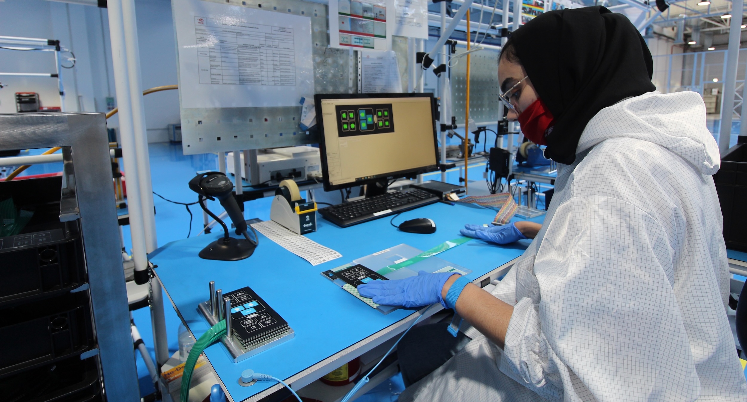
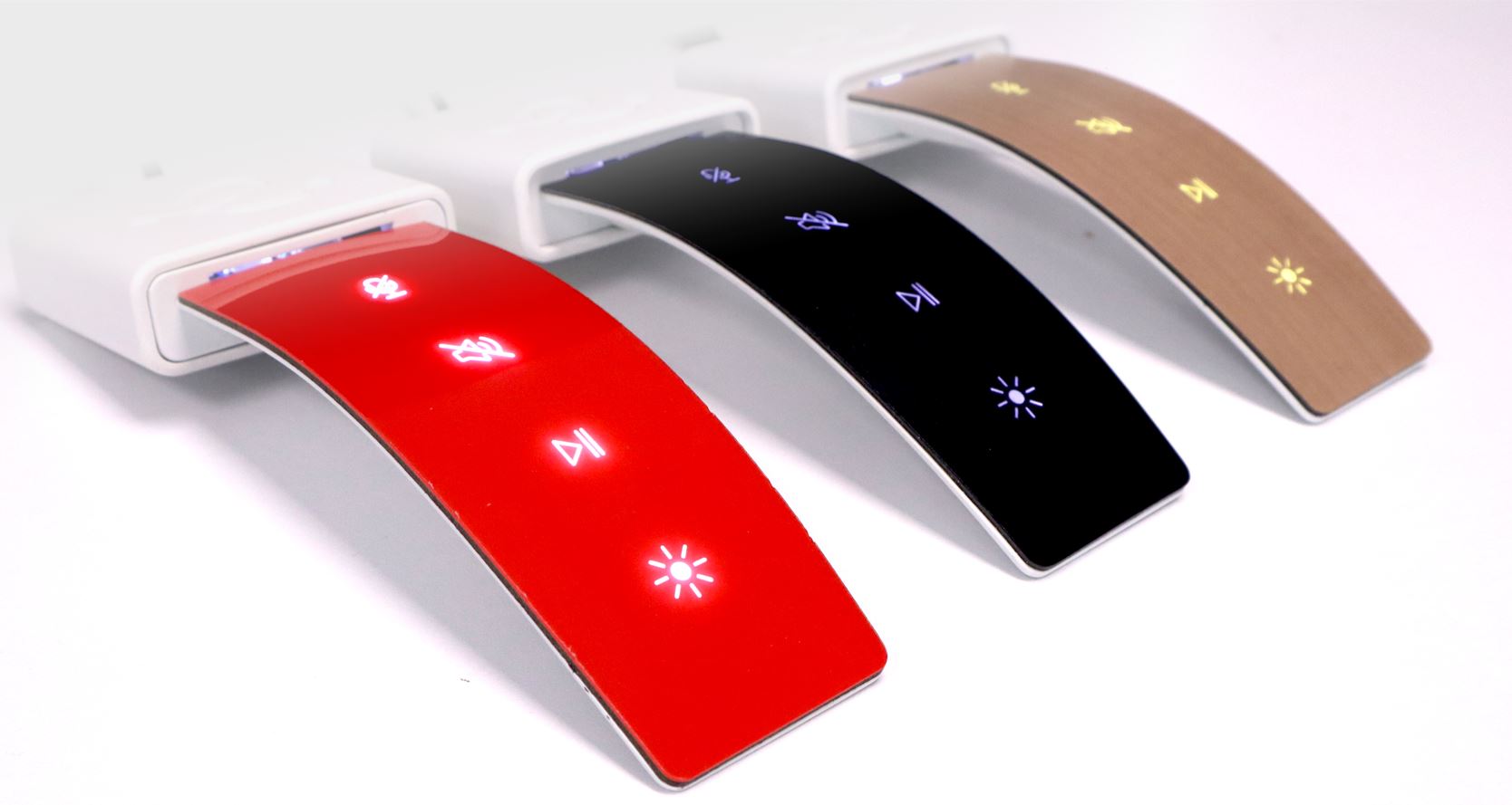
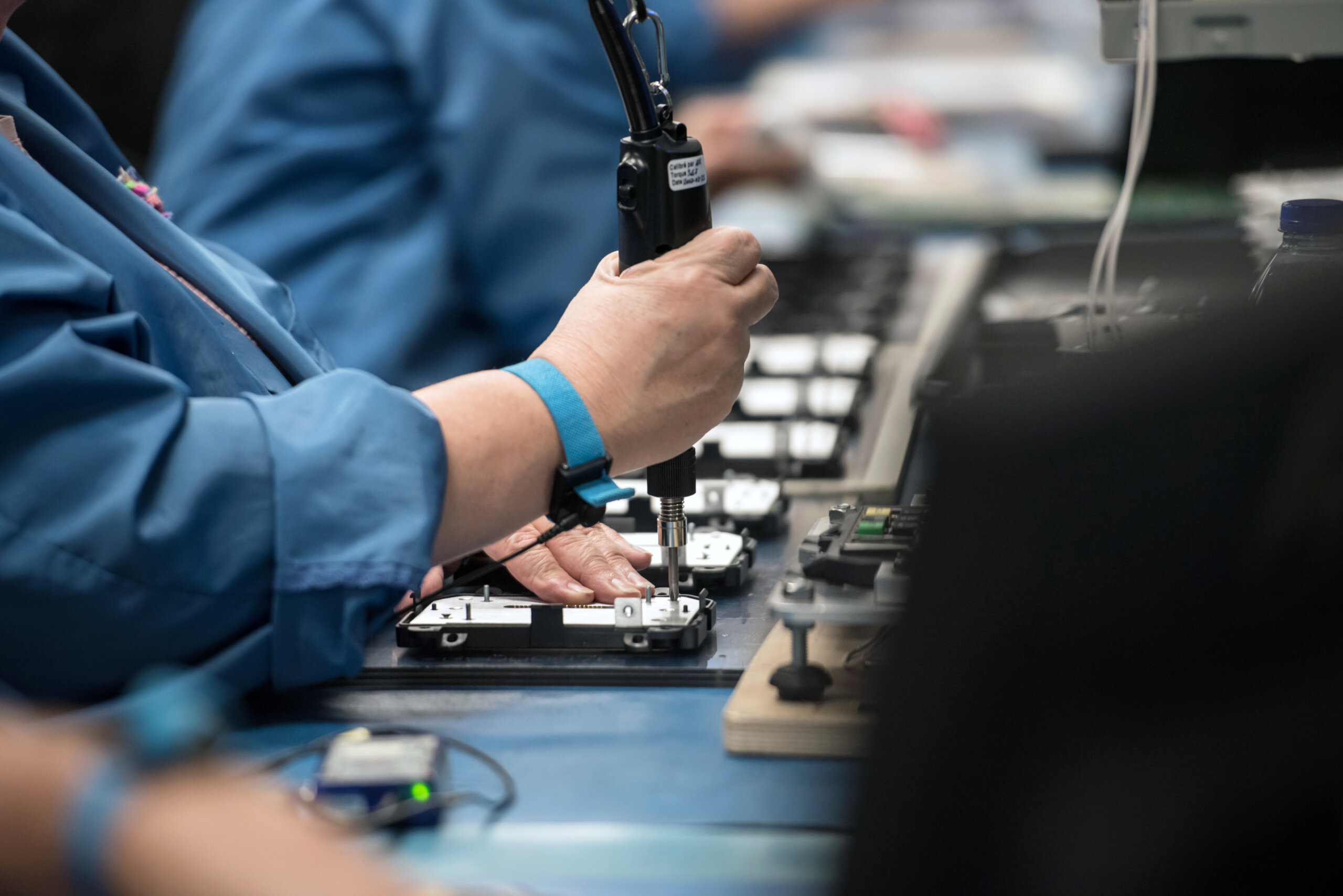
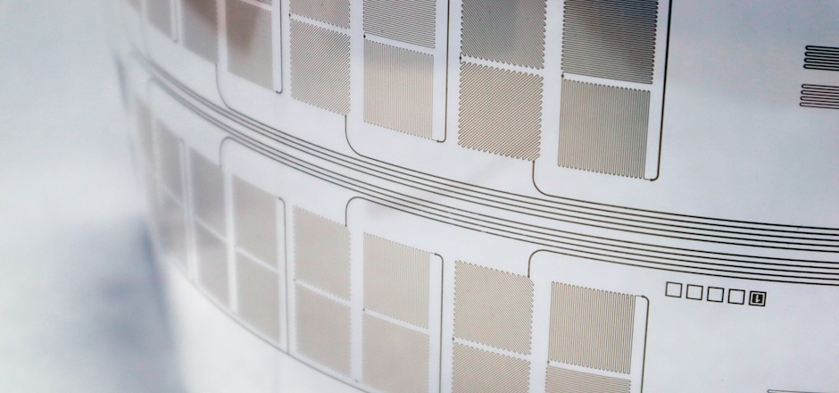
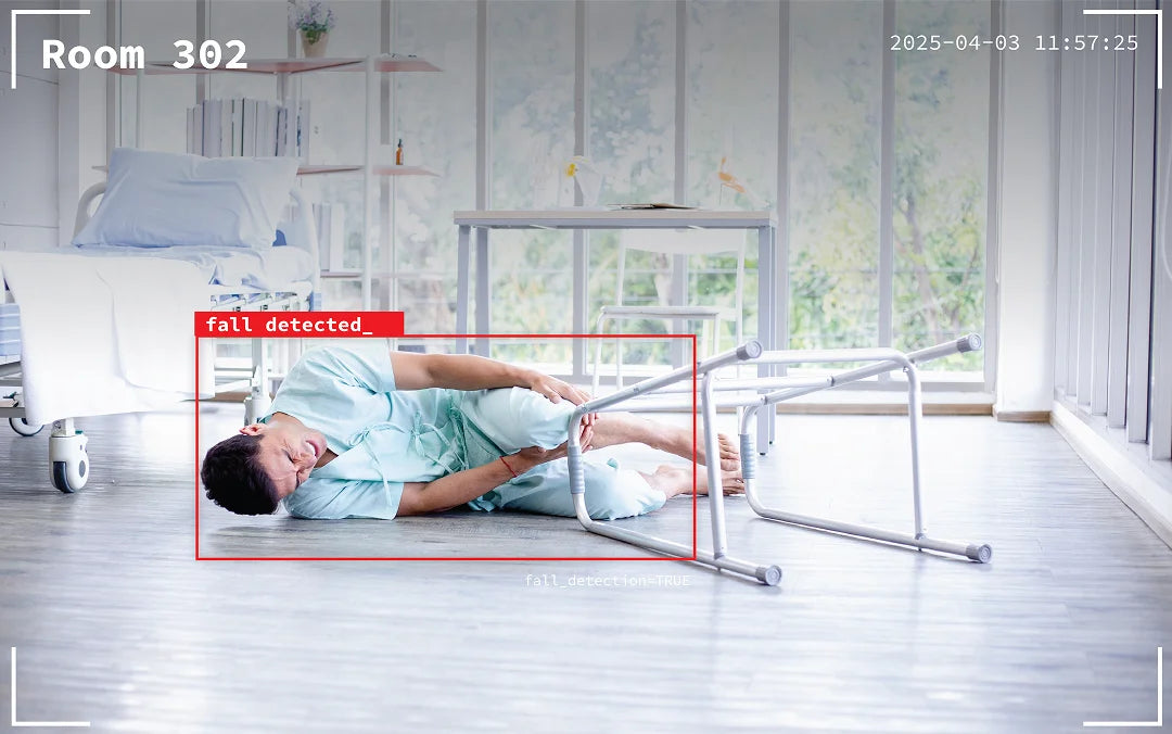
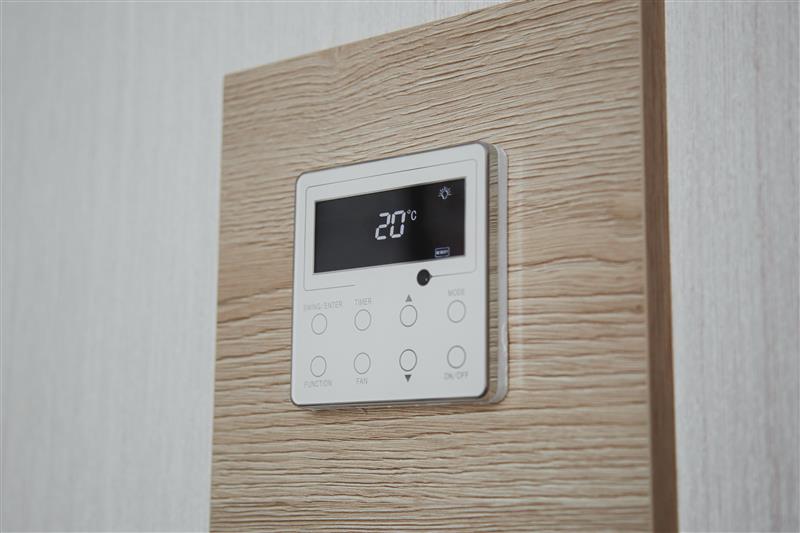
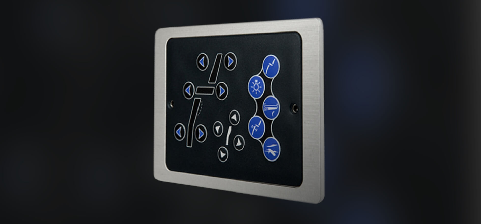
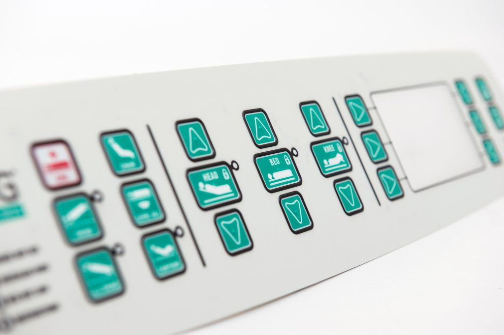
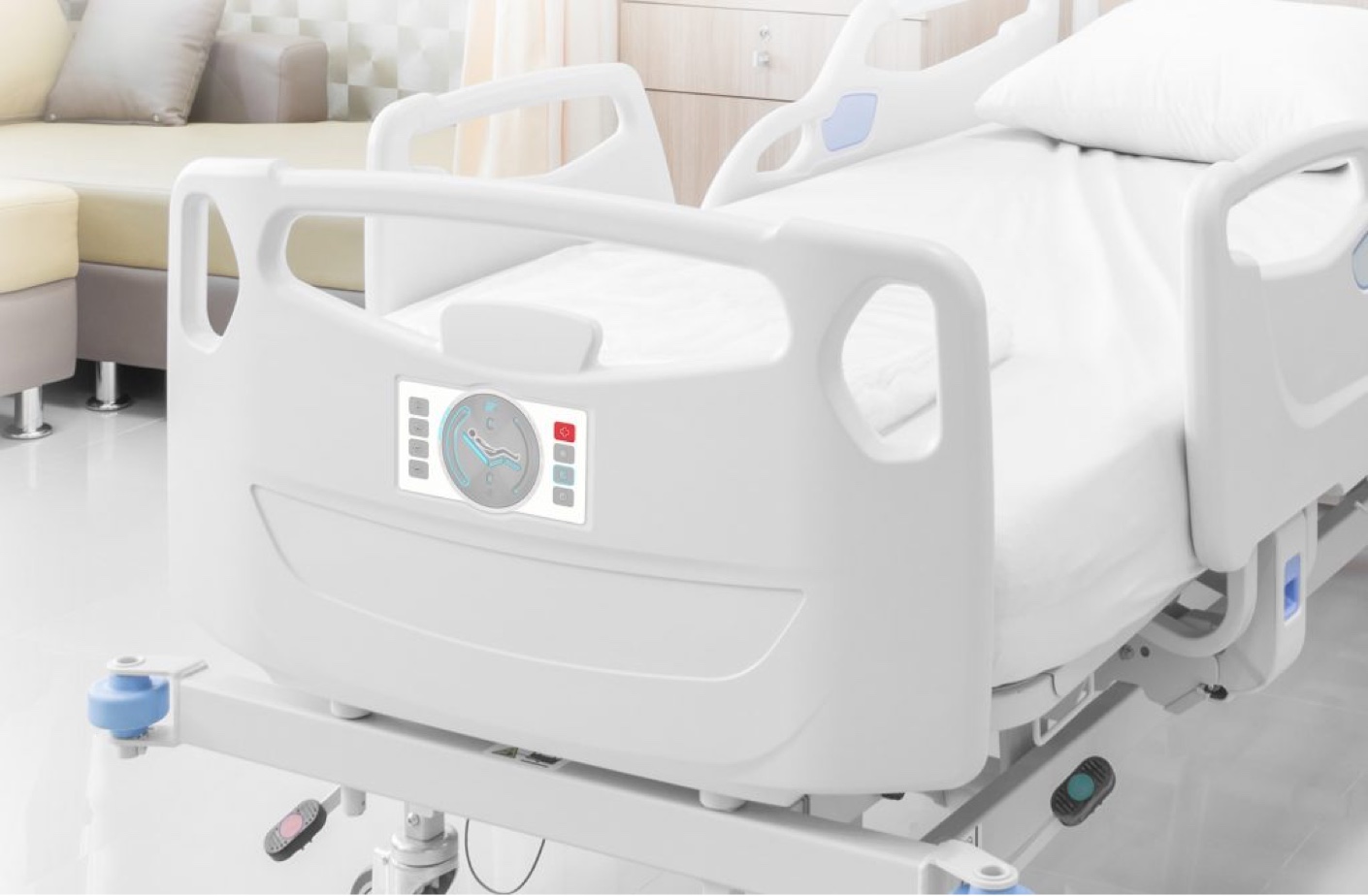
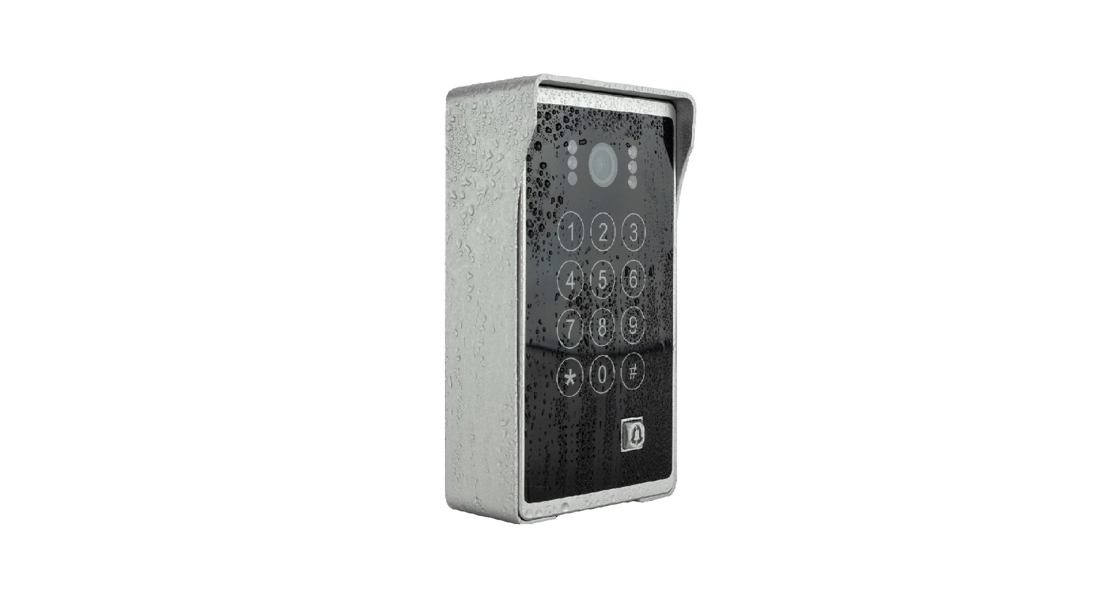
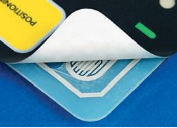
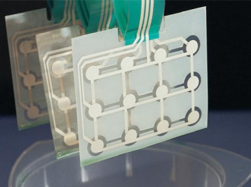
In the ever-evolving world of electronics manufacturing, the functionality of a device is often only as good as its weakest link. For membrane switches and flexible circuits deployed in harsh environments, whether it’s a medical device being continually wiped down with strong disinfectants, an automotive part exposed to gasoline fumes or an aerospace instrument that is subjected to rapid altitude changes, the weakest link they have in common, has traditionally been the adhesive.

For years, Pressure Sensitive Adhesives (PSA) have been the industry standard. While effective for simple applications, PSAs have inherent microscopic flaws that lead to catastrophic failures when pushed to the limit. Enter HeatSeal®, a revolutionary technology that doesn’t just stick layers together, it fuses them. This blog explores why HeatSeal® should be the go-to solution for high-reliability applications and how it solves the critical vulnerabilities of traditional adhesives.

The Micro-Fissure Problem

In order to understand all the benefits of HeatSeal®, we must first understand why traditional Pressure Sensitive Adhesives can fail. Under a microscope, a layer of PSA looks less like a solid wall and more like a sponge. PSAs are “tacky” solids that never achieve 100% wet-out (process of an adhesive flowing to maximize contact area) on a surface. This results in inherent micro-fissures and voids (microscopic air channels that act as potential points of failure.)

These voids create a phenomenon known as capillary action. Like how a paper towel wicks up water, these micro-fissures draw in liquids, cleaners, and chemicals. Over time, this ingress dissolves the bond and attacks the sensitive silver circuitry underneath, leading to electrical shorts and system failure. Furthermore, these air gaps provide low-resistance paths for Electrostatic Discharge (ESD), putting delicate electronic components at risk.

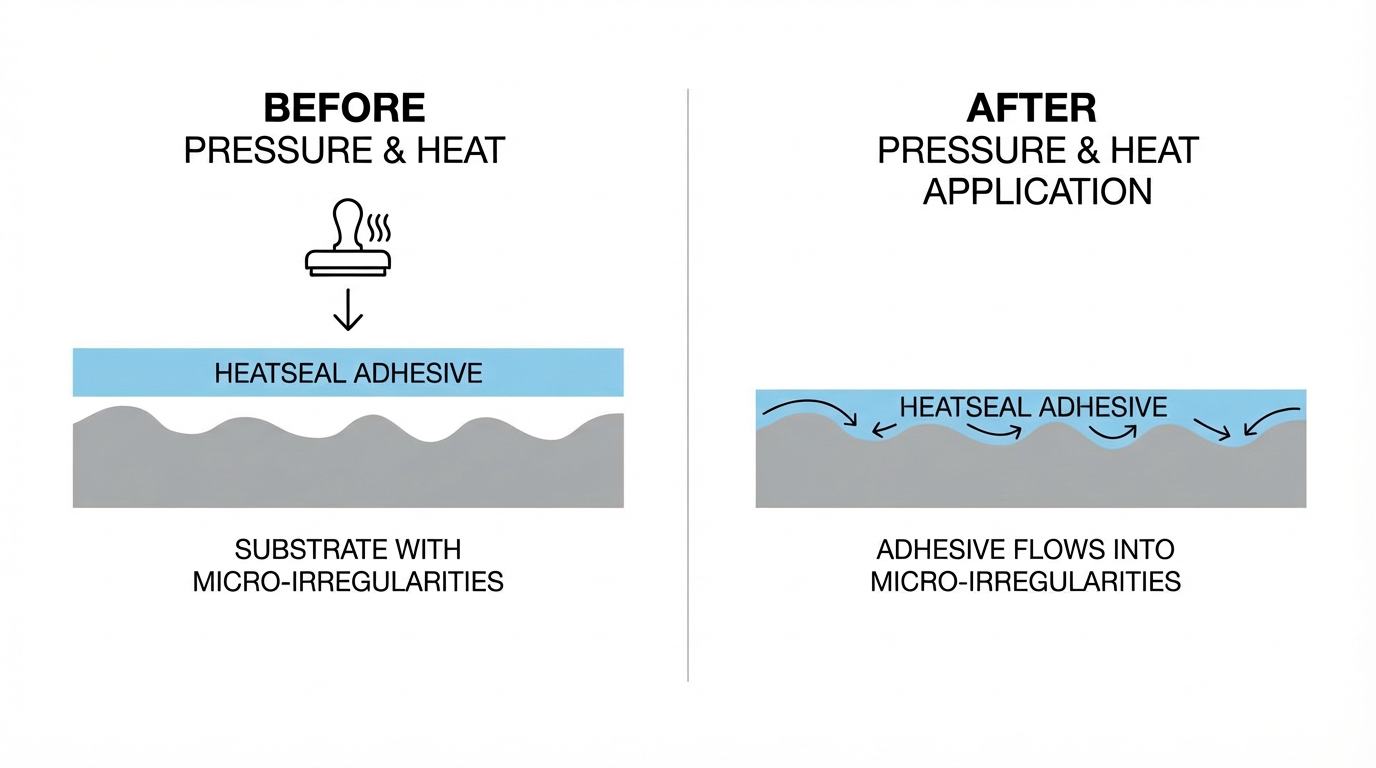
The Power of Thermal Fusion

HeatSeal® fundamentally changes bonding through a process called thermal fusion. Unlike PSAs, which rely on surface tack, HeatSeal® is a proprietary adhesive that transitions to its final state under controlled heat and pressure. During this phase change, the adhesive flows into every microscopic surface irregularity, completely wetting out the substrate. The result is a solid, fissure-free barrier that is chemically and physically fused to the carrier. This eliminates the capillary pathways that plague PSAs, creating a true hermetic seal. It is not merely a glue; it is a structural integration of the switch layers.

Unmatched Chemical Resistance

One of the most significant advantages of HeatSeal® is its resistance to chemicals. In comparative testing, the difference are clear:

  • Household Cleaners: Standard PSAs exposed to common cleaners like 409®, Fantastik®, or bleach often fail within 20 to 40 days due to adhesive dissolution and fluid ingress. In contrast, HeatSeal® switches have withstood over 180 days of continuous immersion with zero degradation.
  • Hydrocarbons and Solvents: Exposure to gasoline causes PSAs to dissolve and delaminate within hours. HeatSeal® maintains 100% insulation resistance and structural integrity even after 14 days of full immersion.
  • Modern Contaminants: Everyday substances like sunscreen and insect repellent (DEET) are surprisingly destructive to plastics and adhesives. HeatSeal® is specifically engineered to resist these modern chemical stressors, passing rigorous automotive standards (GMW14445) where standard adhesives fail after a single cycle.

Thriving Under Pressure (and Altitude)

For devices used in aerospace or high-altitude environments, air pressure differentials are a silent killer. As a device ascends to 40,000 feet, the air trapped inside a switch expands. With PSAs, this air forces its way out through the micro-fissures. The problem arises upon descent: the switch cannot “re-inhale” quickly enough, creating a vacuum that sucks the switch layers together, causing permanent collapse and electrical shorts.

HeatSeal® prevents this “bends” phenomenon. Its hermetic bond prevents air expulsion in the first place. While the switch may bulge slightly at high altitudes, the bond holds firm, and the switch returns perfectly to its neutral state upon return to normal pressure. This capability has been validated in medical and aerospace applications from 100 to 40,000 feet.

Additionally, the mechanical strength of the bond is immense. While industry specifications typically require a switch to withstand 7.5 PSI of internal pressure, we exceed this limit with our HeatSeal® adhesive to an average limit of 35 PSI internal pressure during testing. can assemblies average a burst pressure of 60 PSI—an 8x safety margin that ensures IP67 and IP68 ingress ratings are easily achievable.

Superior Thermal Stability

Temperature fluctuations are the enemy of adhesion. Standard PSAs exhibit a non-linear bond strength that degrades rapidly as temperatures rise. At 100°C, the peel strength of a PSA can drop by over 90%, leaving the assembly vulnerable to delamination caused by the expansion and contraction of different materials.

HeatSeal® maintains a stable bond profile across a massive operating range of -25°C to 100°C. At the 100°C mark HeatSeal® retains above 2.0 lbs/in² of peel strength. This thermal stability ensures that the switch remains intact and functional even in the sweltering heat of an engine bay or an industrial sterilization chamber.

Built-in ESD Protection

Finally, HeatSeal® offers a hidden electrical benefit. Because it eliminates air voids and is composed of high-dielectric polyester resin, the adhesive layer itself acts as a powerful insulator against Electrostatic Discharge (ESD). PSA based switches often require expensive secondary shielding layers, such as printed silver grids, to protect sensitive circuitry from static shocks that travel through the adhesive’s micro-fissures. HeatSeal® inherently provides a minimum of 15kV (and up to 25kV) of dielectric protection, effectively sealing the conductive traces. This not only improves reliability but can also reduce manufacturing costs by eliminating the need for additional shielding components.

Conclusion

In the world of industrial, medical, automotive and aerospace electronics, the cost of failure is too high to leave things to chance. HeatSeal® represents a shift from simple adhesion to structural fusion. By eliminating the microscopic vulnerabilities of PSAs in high demand use cases, HeatSeal® offers a robust, hermetic, and chemically resistant solution that stands up to the most extreme environments.

For engineers and designers looking to future-proof their devices against water, chemicals, heat, and pressure, HeatSeal® is not just an alternative, it is the next phase in the evolution of adhesive technology. For more information please contact us.

e2ip Manufacturing: Precision and Scale Across Continents

e2ip technologies designs and builds advanced human–machine interfaces (HMI), in-mold electronics (IME) and printed electronics solutions. With manufacturing facilities in both Canada and Morocco, we bring consistent quality, fast lead times, and flexible scaling to programs in medical, aerospace, industrial, defense and transportation markets. Our dual-continent footprint, capabilities, and quality systems translate into customer value where manufacturing is only one part of our broader ideation to fabrication offerings.

Why e2ip’s Manufacturing Footprint Matters

Two regions. One standard of excellence. Our North American and North African electronics manufacturing facilities balance timelines, cost, and quality, so your HMI projects stay on track even as demand or market conditions shift.

Canada: Close Collaboration for Complex Builds

Collaborate directly with our engineering and advanced manufacturing teams. Ideal for high‑reliability HMI, IME, and printed electronics projects, that benefit from tight process control, quick iteration, and secure supply chains.

Morocco: Cost‑Efficient Scale Near EMEA

Our Morocco facility provides cost-competitive, scalable production for European markets. Highly capable, this site enables efficient HMI, IME, and printed electronics manufacturing while maintaining consistent quality.

Manufacturing with e2ip offers:

  • Consistent quality HMI, IME, and printed electronics, backed by mature, audited processes
  • Rapid prototyping into scalable production
  • Tight traceability and repeatability for regulated applications
  • A global supply strategy without single‑source risk
  • Direct collaboration between engineering and manufacturing to increase efficiency and cut time‑to‑market

Our Manufacturing Capabilities: What We Make and How We Build

We produce rugged user interfaces and controls that are thin, light, and integrated. Our advanced processes—including printing, molding, assembly, and finishing—are optimized for demanding environments.

Capabilities Include:

  • Advanced printing for conductive and decorative layers in HMI and printed electronics
  • Forming and lamination for complex 3D shapes
  • Precision assembly and sealing for harsh environments
  • Environmental and functional testing aligned to industry standards
  • Designing for manufacturability and continuous process optimization


Quality Systems Built for High-Reliability Applications

From early prototypes to serial production, our processes emphasize repeatability, traceability, and control. The goal is simple, predictable performance, regulatory/certification compliance which results in a smoother experience for our customers.

Program Advantages:

  • Clear transfer from NPI to production with gated reviews
  • Robust change control and documentation
  • Process capability monitoring to sustain yield and reliability
  • Supplier development and incoming inspection for stable inputs

More Than Manufacturing: Ideation To Fabrication

Manufacturing is a core pillar, but only one part of the value e2ip can offer. Our ideation to fabrication method connects early concepting, materials exploration, UX and industrial design, and feasibility testing with prototyping, validation, and full‑scale production in Canada or Morocco. This results in fewer handoffs, lower risk, clearer accountability, and a faster pathway to a shipped product.

Let’s Build What’s Next

If you need new HMI controls for your next project, you’ll find a trusted and reliable partner in e2ip, delivering solutions from ideation to fabrication, built to meet rigorous regulated industry standards. Contact us today to discuss timelines, certifications, and manufacturing solutions.

Train Passenger Experience

Modernizing first-class rail cabins requires innovation to meet rising passenger expectations. This is accomplished by transforming the first-class passenger experience through innovation and design excellence. Integrating smart, space-efficient solutions into cabins delivers greater comfort, personalization, and sustainability. This strategic focus not only enhances the onboard journey but also reinforces brand leadership in a highly competitive market.

Manufacturers must meet strict safety, performance, and interoperability standards.

Key challenges include

Safety and Fire Compliance: Systems must meet FRA regulations and EN 45545 fire protection standards to ensure passenger safety and material reliability.

Environmental Durability: Electronics must withstand vibration, temperature extremes, and mechanical stress.

Design Efficiency: Replacing bulky mechanical controls with sleek, embedded interfaces requires intuitive, space-conscious design.

Technology Validation: Printed and in-mold electronics must pass rigorous testing to prove long-term reliability in transportation environments.

In close, ongoing collaboration with train manufacturers, we explored several innovative interior concepts. The capacitive passenger control unit presented here exemplifies our approach to combining advanced electronics with refined industrial design for seamless Human–Machine Interfaces (HMI).

Using In-Mold Electronics (IME) touch-sensitive controls are embedded directly into thermoformed cabin panels, replacing mechanical buttons with a sleek, durable interface. A compact touchscreen further enhances functionality by displaying travel data—such as time to destination, weather, and ambient lighting—while offering full customization to reflect operator branding and passenger preferences.

Technical Highlights

  • Printed Electronics: Enables thin, flexible integration of electronics directly into the surface using printed conductive inks and adaptable substrates for intuitive control of seat functions, lighting, and blinds.
  • IME Integration: Embeds electronics during molding for a tamper-resistant surface built to transportation-grade durability.
  • Embedded Systems: Low-power microcontrollers support responsive touchscreens with real-time data display.
  • Custom GUI: Interfaces are tailored to operator branding and designed for passenger ease of use.
  • Environmental Testing: Components meet EN 50155 and EN 61373 standards for vibration, temperature, and shock resistance.

e2ip offers a full range of supporting services to ensure successful development and deployment your project. Multidisciplinary design teams guide the process from initial concept to final production. In-house prototyping capabilities enable rapid iteration and testing, while deep expertise in printed electronics and HMI integration supports scalable, cost-effective manufacturing tailored to transportation applications.

If you would like to discuss your project with us please reach here.

Customizable Touch Screens

Touch screen technology has grown far beyond its early use in retail settings, as it now drives communication and control in industrial automation, medical devices, connected workspaces, and more. As technology advances, more organizations are adopting customizable touch screen displays, personalizing user experience across industries.

At e2ip Technologies, we develop smart touch surfaces that merge precise engineering with real-world usability. Every display we build is designed for people first, as we look at how users interact with machines, how touch inputs translate into results, and how technology can adapt to context instead of the other way around.

How Custom Touch Screens Are Improving User Experiences

Adaptive Interface Design

In complex workplaces, information needs to move at the pace of the user. Custom touch screens can easily keep up with most tasks by changing their layouts and settings to reflect that rhythm.

For example, a nurse monitoring vital signs can switch between functions quickly without losing focus, and operators in manufacturing can access key features with fewer steps and less visual clutter. These adaptive interfaces can create an easier flow between user and machine, meaning that tasks are done faster and with less stress.

Branding and Aesthetics

Design tells a story before a word is read or a button is pressed, and by using custom displays, organizations can bring their visual identity directly into the interface. In consumer electronics, this connection strengthens familiarity and trust. Automotive dashboards and kiosks rely on bold designs to show their brand’s quality and reliability, and with these systems, you can integrate brand elements into the interface itself, reinforcing your message at every point of contact.

Multi-Industry Versatility

Custom touch technology delivers dependable performance across a wide range of industries because it can be precisely adapted to specific operational needs. In medical environments, touch interfaces are designed to meet stringent hygiene and safety standards—featuring smooth, sealed surfaces that ensure enhanced durability, easy cleaning, and reliable operation in patient monitoring systems and diagnostic equipment.

In industrial settings, touch screen technologies must perform under demanding conditions such as vibration, dust, moisture, and temperature extremes. Ruggedized capacitive and resistive touch panels deliver consistent performance for operators wearing gloves, while maintaining precise user interaction even in harsh environments. These solutions are often integrated into industrial control systems, where responsiveness, reliability, and long-term durability are critical for continuous operation.

Multi-touch functionality further enhances productivity by enabling intuitive gestures and fluid control on large displays.

Smart System Adaptation

Modern custom screens operate within connected ecosystems that share data fluidly between devices and systems. Their multi touch capabilities and refined gesture recognition create a smooth, natural experience that feels effortless. Designed with durable glass surfaces and tuned touch sensitivity, they hold up under harsh environments without lessening their responsiveness.

Increased Productivity & Engagement

When users feel in control, efficiency comes naturally. A highly responsive screen surface provides precise input and encourages smoother workflows. Built with durable materials and long-lasting performance in mind, these interactive touch screens hold up under constant use without losing accuracy. Their consistent responsiveness builds confidence, helping users focus on results instead of navigation. Each customized solution is adaptable and keeps its dependable quality across every interaction.

Moving Technology Forward with Purpose

At e2ip Technologies, we design and manufacture touch screens that are custom suited for almost any task. Our tailored solutions bring together interface design and human insight to deliver technology that permits an enhanced user experience where it matters most.

Learn more about our smart touch surfaces and explore the pros & cons of touch screens to see how customizable interfaces can meet your business’s specific needs and create lasting value.

Curved Capacitive Switches: Enabling Seamless 3D Surface Integration

Curved capacitive switches are redefining how people can interact with technology. At e2ip technologies, a mainstay of our ongoing efforts to enable greater design freedom and create the interfaces of the future, we’re shaping surfaces that respond as naturally as they look, turning touch into an intuitive experience.

These curved interfaces erase the boundary between design and function, allowing controls to be seamlessly integrated into the contours of a product. From automotive interiors to next-generation consumer devices, they’re changing how user interfaces and technology fits into everyday life.

What You Need to Know about Curved Capacitive Switches

Seamless 3D Integration for Modern Interfaces

Curved capacitive switches eliminate the need for mechanical buttons, putting capacitive sensing directly into the surface itself, resulting in a smoother design with reduced assembly. For example, in a medical device, the seamless stacking of three layers—combined with the absence of creases or moving buttons—creates a unified, sealed surface that is easier to sanitize. What matters most is that every press or tap feels deliberate and consistent, no matter the environment, with reliable detection and control.

Precision Forming Without Losing Performance

Creating a responsive capacitive touch interface that bends without losing uniformity demands tight material control. We counter this through calibrated lamination methods that hold electrical sensitivity steady from edge to edge. This all works to define accuracy, and every part that leaves production delivers the same level of responsiveness, flat or curved, small or large. That consistency allows our partners to build with confidence.

Enhanced Aesthetic and Functional Freedom

When functionality no longer dictates product design, designers gain the freedom to explore new possibilities, and touch zones can emerge through subtle light, pattern, or shift in texture. There is no need for separate components that break up the surface.

With our Capflex®, platform, teams experiment with different geometries and backlighting approaches while keeping accurate feedback, and test every detail for clarity and responsiveness.

capflex capacitive panels

Durability and Environmental Resistance

Longevity depends on more than strong materials; it depends on structure. By removing moving parts, curved capacitive switches reduce wear and mechanical failure. Their sealed layers block out moisture, dust, and debris that often cause problems in standard controls. In aircraft cabin controls or medical systems, that resilience is a necessity.

The multilayer build and conductive films make them robust, durable, and capable of maintaining high utility.

Smart Surface Interaction

A curved capacitive touch switch can do much more than detect a touch, with built-in features such as adjustable lighting,  or variable sensitivity, that help it become a dynamic control surface. For example, an interface can respond differently to a light tap than to a firm press. In other cases, changes are based on user proximity or environmental cues. We work closely with partners to define these behaviors so that every response feels intentional and intuitive, not pre-programmed or generic.

Rethinking the Future of Interaction

Our work in curved capacitive switch technology is driven by making things feel more natural. The answer often begins at the material level, where printed electronics meet advanced surface design. Through products, services, and continuous research, we build interfaces that react with precision. Each collaboration combines engineering insight with practical experience gained from decades in the field. For teams building the next generation of connected products, we provide the expertise and manufacturing capability to turn vision into dependable, intelligent surfaces.

From Ideation to Fabrication: A Clear Path with E2IP

At e2ip technologies, we understand that taking a product from concept to market is fraught with challenges. It calls for more than technical expertise. It requires a strong grasp of what customers want to achieve and how end users will interact with the final design. Nowhere is this more critical than in Human-Machine Interface (HMI) solutions, where performance, usability, and design freedom need to come together.

Our “ideation to fabrication” approach addresses this complexity head-on. By combining design, engineering, prototyping, testing, and certification under one process, we help organizations maintain momentum through each stage.

Leveraging decades of expertise across aerospace, medical, defense, transportation, and industrial markets, e2ip provides clients with both confidence and clarity. From ideation workshops to certified manufacturing, our process ensures your ideas are transformed into fully validated and deployable innovations.

Why Peace of Mind Matters

Everyone knows that uncertainty slows innovation. Is the idea feasible? Can it be manufactured at scale? Will it meet aerospace, medical, or defense compliance standards? These questions can delay critical business goals.

e2ip mitigates these risks by placing multidisciplinary teams at the center of each project. Engineers, scientists, and designers work within a proven framework that delivers visibility, accountability, and confidence—so leadership teams know programs are progressing toward measurable outcomes.

A Structured Path to Success

1. Project Management with Precision

Every engagement follows a five-phase model: launch, planning, execution, monitoring, and closure. Clear KPIs track cost, timing, and quality, ensuring decision-makers benefit from transparency and predictable delivery at each stage.

2. Ideation and Design

In the ideation phase, creativity and technical feasibility intersect. Through brainstorming, sketching, mock-ups, and prototypes, e2ip helps organizations rapidly define the best direction. This structured method of thinking lays the foundation for innovation that is both visionary and manufacturable.

design sketch

3. Prototyping Services

Our prototyping services ensure that Human-Machine Interface design & engineering decisions can be validated early in the process. A digital model can only go so far; holding a mock-up or testing a functional build gives leadership teams a chance to judge form, fit, and usability for themselves, while also making it easier to identify potential opportunities or risks that weren’t apparent earlier. This early interaction often shapes better decisions and keeps projects moving in the right direction.

4. Engineering & Manufacturing Excellence

With deep expertise in industrial, electrical, mechanical, and software engineering, e2ip delivers integrated product development services. Our capabilities include PCB assemblies, embedded firmware, systems architecture, circuit design, optical simulation, and stress analysis. Clients benefit from end-to-end engineering that reduces technical risk.

worker assembling a product

Manufacturing is executed at certified plants in Canada and Morocco, operating under AS9100 and ISO 13485 standards. From injection molding to tactile keypad optimization and low-pressure molding, e2ip ensures designs scale into reliable, certifiable solutions built for global markets.

5. Certification Support

For more than 40 years, e2ip has simplified compliance for highly regulated industries. We deliver qualification test plans, certification documents, prototype testing, materials analysis, and conformity inspections in partnership with accredited laboratories. This embedded regulatory expertise ensures clients enter markets with confidence.

Core Capabilities: From Printed Electronics to IME

e2ip’s portfolio goes beyond services—our expertise in printed electronics and in-mold electronics (IME)accelerates innovation across industries. Technologies such as conductive inks, Lumifilm® lighting, HeatSeal® adhesives, heating solutions, and printed sensors provide building blocks for next-generation Human-Machine Interfaces.

Together with advanced solutions like Smart Structural Surfaces™, Smart Touch Surfaces, and electromechanical systems, e2ip delivers functionality without compromising industrial design freedom. This unique convergence of design aesthetics, usability, and engineering rigor positions our clients ahead of the curve.

The e2ip Advantage

Customers trust e2ip because we align strategy with delivery. Advanced technologies are embedded directly into product design—whether tactile interfaces, smart surfaces, or complex electromechanical platforms. Solutions are not only innovative but also intuitive, robust, and scalable.

e2ip delivers:
– Proven cross-industry expertise in aerospace, medical, defense, transportation, and industrial markets
– Comprehensive product development services from ideation through certified fabrication
– Manufacturing in AS9100 and ISO 13485 certified facilities
– Rigorous mechanical, electrical, and software engineering capabilities
– Accelerated prototyping and validation processes
– A partnership approach that enhances ideas without diluting intent

With e2ip, innovation is reliable, compliant, and designed to generate long-term business value.

Ready to Transform Vision into Reality?

If your organization is ready to turn strategic ideas into commercial products, e2ip offers the expertise, infrastructure, and certified processes to deliver. Whether your focus is Human-Machine Interface design, printed electronics, or smart surface integration, we transform vision into scalable solutions. Contact Us.

What Industry 4.0 Really Means

People like to throw the term around, but in practice, what Industry 4.0 really means is decisions made in real time and acted on in real time. Machines, systems, and operators all working from the same live data, without waiting for someone to pass along a note or hold a meeting.

It’s not complicated to picture. A camera spots a defect before the next part leaves the station. A machine makes a micro-adjustment on the fly. A supply chain reroutes product before the shortage even hits the loading dock. According to the Industry 4.0 BDC reports, the expectations around Industry 4.0 adoption have huge implications.

What Is Industry 4.0?

The history matters here. The First Industrial Revolution was all about steam engines driving the looms, pumps, and presses that finally pulled production out of small workshops and into purpose-built facilities. The Second Industrial Revolution brought electricity and assembly lines, turning factories into high-output operations capable of mass production on a scale no one had seen before. Then came the Third Industrial Revolution, often called the “digital revolution” when electronics and computers became ubiquitous everywhere from the sales office to the factory floor reshaping how work was done, cutting manufacturing process labour needs in some areas while boosting precision and speed in others.

Now we’re in the Fourth Industrial Revolution (Industry 4.0), where smart and autonomous systems are quickly making their way into production lines, and other business processes, with profound effect.

It’s not just automation, it’s smart manufacturing: machines, sensors, and artificial intelligence connected into a single nervous system that can see, think, and act. This is where cyber-physical systems bridge the gap between the physical world of machines and the digital technologies that drive them. It’s digital transformation at its most tangible.

The vision of a smart factory today is one where the production process is augmented by machine learning from its own data, adapts processes in real time, and integrates with supply chain and design systems. The physical and digital layers move together, as if they were built as one.

Advantages of Industry 4.0

The advantages of Industry 4.0 aren’t hypothetical. They’re measured in manufacturing efficiency; hours of uptime, percentage points of yield, and fewer pallets of rework sitting by the scrap bin.

Predictive maintenance is a simple example. Instead of letting a worn bearing wreck a line mid-week, you swap it during a scheduled stop. Same with automated inspection. Catch the flaw as it happens and adjust, rather than producing a day’s worth of bad product.

That’s where our Edge AI Sensing Kit pulls its weight. It’s compact. Runs on little power. Has a high-sensitivity camera sensor feeding a neural processor that chews through vision data right there on the floor. No cloud hand-off, no bottleneck. You can load it with YOLO or a custom model, point it at a process, and it starts delivering results before anyone’s had time to print a dashboard.

Challenges for Industry 4.0

All the new technologies that are contributing to Industry 4.0 aren’t magic switches.

Some of your gear can’t talk to anything modern without retrofits. That costs. People won’t trust new systems overnight. Cybersecurity can’t be an afterthought when every extra device is a possible entry point. And yes, capital budgets are always tight, even when the math says the payback’s there.

The fix? Start small. Pick a point where you know an improvement will show up on the balance sheet fast.

Big Data: Challenges and Opportunities

Industry 4.0 isn’t just about sensors and robotics — it’s about the way we analyze data and act on it. Cloud computing connects plants to centralized intelligence, while additive manufacturing puts complex parts into production without the usual lead times. With better data analysis and big data feeding decision-making, it’s possible to design more efficient manufacturing processes and fine-tune existing ones to be a truly efficient.

Advanced technologies like enterprise resource planning systems tied to real-time data analytics make it possible to see the whole operation in one view, from raw materials to delivery. Programmable logic controllers remain the backbone on the floor, but embedding programmable logic controllers into smart machines now adds adaptability that wasn’t there before. The goal is to optimize processes using everything from advanced simulation software applications to tighter supply chain management. The result? An efficient supply chain that moves with the same speed and accuracy as the production line.

In a digital manufacturing setup, production data flows through mobile devices, control stations, and planning systems without delay, keeping every level of the operation working from the same real time data.

How e2ip Is Building the Future of Digital Transformation

Rolling out Industry 4.0 isn’t a one-shot overhaul. It’s a series of wins. You fix the obvious pain points first and then build from there.

That’s our approach with partners. Solve the pressing problem, prove the result, and connect those wins into a system that’s faster, smarter, and harder to break. The Edge AI Sensing Kit is often the first piece in that puzzle. Quick to deploy. Easy to adapt. Capable of changing the economics of a process almost overnight.

If you’ve got a weak link in production, we can shore it up. If your visibility ends halfway down the line, we can extend it. Contact us and we’ll figure out where Edge AI and our SMART STRUCTURAL SURFACES™  can help your operations the most.

E2IP’s Molecular Ink and its Role in SMART STRUCTURAL SURFACES™

Introduction

e2ip products are at the forefront of printed electronics and as the demand for smaller, more functional, and aesthetically pleasing electronic devices grows, the need for innovative materials and manufacturing techniques becomes increasingly important. e2ip utilizes a variety of conductive inks such as nanoparticle inks, flake inks, including their patented molecular ink (MINK), developed in collaboration with the National Research Council of Canada (NRC)

Their team is committed to providing optimal solutions for each application by determining the most suitable ink selection based on the design requirements and rheological properties. By leveraging the unique properties of each ink type, e2ip products offer unparalleled functionality, adhesion, durability, and performance in the printing process, making this technology an ideal choice for a wide range of electronic applications. This commitment is further exemplified through the use of molecular inks and their role in smart structural surfaces, where they enable seamless integration of electronics into complex, functional designs. 

The Innovation Behind e2ip’s Molecular Ink

Conductive inks are engineered by binding polymers and conductive materials, resulting in inks that deliver high electrical conductivity, flexibility, and formability.  Unlike traditional flake inks, e2ip’s MINK is based on ionic molecules, offering superior conductivity, elongation, and compatibility with a wide range of printing techniques such as screen printing and inkjet printing. This innovation, developed in collaboration with the National Research Council of Canada (NRC), addresses the limitations of conventional inks. 

Key Benefits of Molecular Ink:

  • High Electrical Conductivity: Ensures reliable performance in demanding electronic applications.
  • Formability and Flexibility: Allows for seamless integration into curved and freeform surfaces, supporting advanced design freedom, during the thermoforming process.

Enabling SMART STRUCTURAL SURFACES™ 

SMART STRUCTURAL SURFACES ™ represent a leap in human-machine interface (HMI) design by embedding electronics directly into the structure of surfaces. This methodology eliminates the need for bulky control panels and tech boxes, enabling sleek, lightweight, and highly functional products.

SMART STRUCTURAL SURFACES™ are used in a variety of sectors, from automotive interiors and aircraft armrests to medical devices and home appliances. They enable intuitive, touch-based controls and seamless integration of lighting, sensors, and antennas, all within a single, lightweight unit. This not only improves user experience but also supports space and weight savings and cost-effectiveness.

How Molecular Ink Enable SMART STRUCTURAL SURFACES™:

  • Printed Electronics as the Core: The electronic circuitry in SMART STRUCTURAL SURFACES™ is printed using e2ip’s conductive ink, reducing the number of parts and overall device size.
  • Design Freedom: The flexibility and formability of the ink allows electronics to be integrated into curved, freeform surfaces, supporting ergonomic and minimalistic designs while maintaining printing quality.
  • Streamlined Manufacturing: The ink’s compatible nature with various printing and forming techniques simplifies assembly and reduces costs.
  • Aesthetic and Functional Integration: By embedding electronics into the surface, designers can create products that are both visually appealing and highly interactive, with improved touch performance and ease of cleaning.

Conclusion

e2ip’s molecular ink is a foundational technology that enables the creation of SMART STRUCTURAL SURFACES™, redefining what is possible in product design and human-machine interaction. By combining high performance, flexibility, and sustainability, the ink empowers manufacturers to deliver the next generation of intelligent, integrated, and aesthetically pleasing products.

For more information, visit e2ip’s Molecular Ink and  SMART STRUCTURAL SURFACES™.

Edge AI Industry Applications

At e2ip, we’re not just watching the rise of the global Edge AI market—we’re shaping how it gets applied. Across sectors like manufacturing, healthcare, and smart infrastructure, Edge artificial intelligence is helping systems respond faster, use data more efficiently, and reduce their dependence on cloud resources.

Recognizing its diverse applications and sensor needs, e2ip partnered with ST and Siana to launch a machine vision Edge AI Sensing Kit. This kit allows potential customers to test its capabilities in their own settings.

What Is Edge AI?

At its core, Edge AI technology uses a compact, powerful, low-power AI processor, meaning it runs AI algorithms directly on the devices that collect data—like sensors or cameras—without needing to send everything back to a centralized server. The Edge AI processes data locally until a programmed trigger is met, then it alerts the central server about a specific situation.

These devices analyze and act on data where it’s created, which makes a big difference in environments where bandwidth is limited or speed is critical. Edge devices have a low power draw and on-device processors that handle complex AI tasks and learning with limited server communication, reducing bandwidth costs.

Applications and Use Cases of Edge AI

Smart Surveillance

Consider an Edge AI device enhancing a security camera monitoring building access points. The device continually monitors and analyzes people in the area. Constant reporting to headquarters when a person is detected is unnecessary and increases bandwidth costs. An Edge AI enhanced camera analyzes visuals on the device and, when a trigger is met, alerts headquarters about the situation at the access point. It can also enact required steps, such as capturing recordings before the event, tagging the event, and contacting the security team. This is a key application of Edge Computing AI for enhanced security.

Predictive Maintenance in Manufacturing

Another example is predictive maintenance. Here, an Edge AI device can be attached to a vibration sensor within an engine or manufacturing equipment. The AI-enabled device continually monitors vibration levels. While a standard device alerts at a threshold, Edge AI intelligently monitors vibrations, learning patterns and making associations. In this scenario, Edge AI uses vibration patterns and historical data for predictive maintenance, identifying potential issues in expensive engines and equipment pre-emptively to reduce downtime, repairs, and replacement costs. This demonstrates the power of Industrial IoT and Machine Learning at the edge.

Medical Devices

An example of another possible application of Edge AI is in the medical technology market, specifically with patient monitoring devices, both bedside and personal. Integrating an Edge AI processor into a personal medical device, like an insulin pump/monitor, could greatly improve its capabilities and the quality of life for the user and their medical professional. It allows the device to learn about the wearer, tracking patterns and anticipating highs and lows before they become issues. For users followed by a medical professional, it provides more insight and critical alerts without an inundation of excessive information. This highlights the potential of Healthcare AI and Embedded AI in Medical Devices.

The Benefits of Edge AI

Real-Time Processing with Local Intelligence

Edge AI is transforming how organizations approach data processing—offering faster insights, lower latency, and more efficient system behavior. Unlike traditional cloud computing models, where devices depend on remote cloud servers, Edge AI handles local processing at the device level. This shift allows systems to analyze data in real time, enabling faster response times and more agile AI implementation.

Protecting Sensitive Data and Reducing Bandwidth

By processing data directly on-device, Edge AI reduces the volume of unnecessary data transfer, helping organizations maintain tighter control over sensitive data. In use cases like smart security devices or wearable devices, Edge AI’s ability to keep information local not only speeds up performance—it also enhances data security by minimizing exposure and reliance on third-party infrastructure.

Operational Efficiency and Cost Savings

With less dependence on the cloud for processing and storage, organizations benefit from measurable cost savings. Edge AI minimizes the need for constant data transfer and optimizes network usage. It also supports machine learning models that evolve over time, learning from conditions on the ground and adapting without needing to offload computation. This kind of efficiency is especially valuable in high-volume environments or remote deployments.

Intelligent Monitoring and Predictive Capabilities

In industrial applications, Edge AI improves both performance and oversight. From quality control to environmental sensing, Edge AI plays a key role in identifying issues as they happen. It supports real-time analytics and enables integrating intelligent data collection across connected systems. For operations with limited infrastructure, the ability to make decisions independently of cloud access ensures reliability and responsiveness.

A Scalable, Secure Future

Whether deployed in healthcare, manufacturing smart mobility or other applications, Edge AI addresses the growing demand for secure, autonomous, and scalable systems. By bringing intelligence to the edge, edge computing solutions overcome the limitations of cloud-based AI, delivering greater agility, reduced risk, and enhanced performance at the edge. For forward-looking organizations, Edge AI represents a practical and strategic step toward the future.

See What’s Possible

If you’re exploring how machine vision-based Edge AI can enhance your product, process, or prototype, our Edge AI sensing kit is an excellent place to start.

With built-in support for local processing, the kit enables devices to run AI models for tasks like object detection, event recognition, and real-time analytics. It’s a great way to understand how Edge AI technology behaves under actual operating conditions—whether you’re developing for industrial environments, smart infrastructure, or medical monitoring systems.

Need help evaluating fit or planning an integration? Contact our team—we’re here to support your journey.

Out of Sight, In Control: Bringing IME to the Smart Home Controls

The smart home revolution is accelerating. From intelligent thermostats and lighting systems with smart light bulbs to connected appliances and home security devices with wi-fi connected motion sensors, today’s smart home is more interactive and efficient than ever. At the center of this evolution lies the Human-Machine Interface (HMI)—the point where people and smart home tech connect. Yet as innovation pushes forward, traditional switches, knobs, and even basic touchscreens feel increasingly outdated.

Enter In-Mold Electronics (IME), a transformative technology, and ready to help redefine how we interact with the smart devices within our homes. Combining its manufacturing expertise, in IME, through Smart Structural Surfaces™ and proprietary technologies like LumiFilm®and HeatSeal™, e2ip is at the forefront of this transformation.

What are In-Mold Electronics (IME)?

Imagine your smart home device control panel is no longer a bulky bolt-on box but a seamless part of the product’s surface. With IME, controls, lighting, and indicators are fully integrated into the structural surface of the product itself.

IME is a cutting-edge manufacturing process that embeds electronic components—such as LEDs, capacitive sensors, and printed circuitry—directly into thin films. These films are then thermoformed and injection-molded into durable, 3D structural components. Unlike conventional interfaces, which require separate circuit boards and wiring, IME delivers a single unified unit that merges both interface and structure.

This evolution builds upon traditional In-Mold Decorating (IMD) but enhances it by embedding electronics, not just aesthetics.

The IME Advantage: Smarter Design for Smart Homes

Design Freedom 

IME allows for smooth, curved, and visually unified surfaces—ideal for smart home control panels, security cameras, and other devices that demand minimalism and modern aesthetics. Gone are the clunky bezels and physical buttons of the past.

Superior Durability & Reliability

With no exposed seams or mechanical buttons, IME components are naturally resistant to scratches, spills, dust, and wear. Protected by sealed plastic, the embedded electronics inside offer long-term reliability—a critical advantage for devices like a smart lock at the front door or a smoke alarm in the kitchen.

Space & Weight Savings

By eliminating redundant components like circuit boards and connectors, IME reduces the footprint and energy consumption of smart home devices. The result: thinner, lighter, and more power-efficient designs that improve both sustainability and manufacturing economics.

Intuitive Functionality & Improved User Experience

From touch sliders and buttons to proximity sensors and haptics, IME enables rich interaction in a clean, modern surface. Backlit icons and indicators powered by LumiFilm® enhance usability, even in low-light conditions—perfect for home automation systems or lighting controls in hallways and bedrooms.

Easy Maintenance

With no crevices to trap dust or grime, IME-based interfaces are incredibly easy to clean—making them ideal for appliances, bathroom tech, and devices near cooking surfaces.

Simplified Assembly & Potential Cost Savings

Fewer parts mean fewer steps. Integrating multiple components into one smart structural surface streamlines production and can reduce overall costs while improving design flexibility.

Sustainability by Design

IME can significantly cut down on plastic usage and reduce waste compared to traditional multi-part builds—important for eco-conscious brands targeting energy-efficient and environmentally responsible smart home solutions.

Why e2ip Leads in IME for the Smart Home

As a leader in advanced HMI and printed electronics, e2ip brings unmatched expertise in IME implementation for smart home technology.

Their flagship offering, Smart Structural Surfaces™, combines embedded controls, lighting, and connectivity in thin, attractive, and durable 3D panels. From kitchen appliances to smart home control panels, this solution removes the need for boxy enclosures and introduces streamlined, responsive surfaces. It’s ideal for any application where security, ease of use, and visual appeal matter.

Explore our other services to see how e2ip supports smart home innovation from concept to production.

The Enabling Technologies: LumiFilm® and HeatSeal™

LumiFilm®

LumiFilm® is a flexible light guide film that distributes LED light evenly across the HMI surface. It ensures uniform backlighting for icons, indicators, and text—free from hotspots. It’s especially effective in smart lighting, remote control, and audio interfaces where users might want to play music, adjust lights, or check status via subtle indicators.

HeatSeal™

HeatSeal™ is a thermal bonding process that creates a secure, molecular-level seal within HMI assemblies. This technology ensures long-term protection against moisture, cleaning chemicals, and thermal stress. Devices using HeatSeal™ can meet IP67/IP68 standards, making them ideal for moisture-prone environments or heavily used locations.

Why Choose e2ip for Smart Home Devices?

  • Proven Expertise: e2ip has delivered ruggedized HMIs for sectors where failure isn’t an option—medical, aerospace, industrial—and applies that standard to smart home products.
  • Integrated Solutions: From design to production, e2ip provides complete support, including LumiFilm® and HeatSeal™ integration.
  • User-Centric Design: Interfaces are built around how real users interact with connected devices—from adjusting lights, checking a security feed, or letting a family member in through a smart entry system.

The Seamless Future of Smart Home Control is Here

In-Mold Electronics is no longer just a forward-thinking concept—it’s a practical, proven solution for making smart home devices cleaner, stronger, and more responsive. In a competitive market driven by performance and design, IME gives manufacturers the edge to build interfaces that are intuitive, secure, and built to last.

Our Smart Structural Surfaces™, enhanced with LumiFilm® and HeatSeal™, are helping bring IME to the smart home in ways that are as beautiful as they are functional.

Whether you’re designing for next-gen appliances, control panels, or connected systems, e2ip offers a comprehensive approach that goes beyond IME. Explore our other services to see how we support innovation across HMI, printed electronics, and advanced manufacturing.

Looking to bring seamless control and advanced user interaction to your next product? Contact us to explore how we can help you lead the future of home automation.

What You Need To Know About Tactile And Non-Tactile Membrane Switches

All about membrane switches

The first real membrane switches came to market in the early 1980s. But like many innovations, when they were first introduced they were believed to be less efficient. Material was brittle and they were considered a cheap solution because the switch and keyboard didn’t cost very much to manufacture. However, membrane switches and keyboards have undergone many improvements and today are used in a myriad of electronic devices because they have a sturdy user interface. They offer various advantages to the end user and have become indispensable in many industries.

You’re probably familiar with membrane switches on calculators, remote controls, and electronic locks. In contrast to mechanical switches that contain copper and plastics, membrane switches consist of several layers of printed circuits on film. They come in tactile and non-tactile forms that many industries have benefited from, particularly because membrane switches take up less space than their mechanical alternatives.

Tactile Membrane Switches

Tactile membrane switches are most commonly used because they deliver feedback to the user after being pressed. The buttons on the switch have a graphic overlay that has symbols or icons, such as the numbers on a keypad. A tactile membrane switch contains metal domes that push against a conductive footprint when the user presses on the buttons; this spurs an action.

The medical, aerospace or transportation industries have adapted tactile membrane switch technology into their devices because it allows for a smaller amount of components, can be integrated into portable devices, and is lightweight with optimal visibility.

As an example, you will find membrane switch technology throughout medical facilities, including:

  • Hospital bed controls
  • Ultrasound systems
  • Thermostats
  • Patient monitoring equipment

Membrane switches are also commonly used in the aerospace industry. They can be integrated into:

  • Seat controls
  • In-flight entertainment
  • Passenger control units (signage, mood light etc)

When membrane switches are used in the medical industry, they are vulnerable to an assortment of elements such as bacteria, mildew, and cleaning products. That’s why e2ip technologies uses anti-microbial materials when designing and manufacturing hospital bed controls for the benefit of the environment, as well as the patients and healthcare providers. Our experts ensure that membrane switches are also designed for a long life cycle so the controls won’t fade with continual use.

Non-Tactile Membrane Switches

Non-tactile membrane switches are self-contained units and do not provide a high level of feedback, so they are often paired with an auditory signal or visual display to facilitate ease of use. However, they are remarkably cost-efficient and perfect for flat and thin surfaces. A common example is a non-tactile keypad on microwaves that uses an auditory signal to indicate it received your request. Designers and engineers prefer this type of membrane switch because it allows for keypad shaping and sizing customization.

Applications

The transport industry utilizes non-tactile membrane keypads, which are found on their vehicle’s speedometer and at gas stations. The indicators of gas level and speed do not require any tactile action, but the user of a vehicle needs to know and clearly see these levels as they drive. e2ip technologies  provides non-tactile membrane switches with embossed windows and backlighting by LEDs to clearly indicate status.  These types of keypads are cost-effective with user-friendly designs.

e2ip technologies  specializes in custom membrane switches to ensure their integration into any product application for the medical, aerospace, industrial, transport, and defense industries. We strive to develop and improve leading-edge technological solutions on a global scale. Contact us today by calling 1-866-631-6662 or filling out our online request

Adhesive & Bonding Solutions: Why HeatSeal™ is the Superior Choice for Membrane Switch Applications

In our experience working with original equipment manufacturers (OEMs), we’ve seen firsthand that adhesives are more than just a means to bind components. For us at e2ip technologies, we understand that when it comes to membrane switches and printed electronics, it’s about securing long-term reliability, especially in demanding environments. Whether it’s extreme temperatures, harsh chemicals, or persistent moisture, these are the very challenges where traditional adhesives can fail, and product performance is put at risk.

That’s why we developed HeatSeal™. It’s not just another adhesive solution—it’s one designed to thrive where others break down. OEMs rely on their products to perform in the real world, and we made sure HeatSeal™ offers that reliability, ensuring your products are protected even in the toughest conditions. HeatSeal™ doesn’t just hold things together; it safeguards the integrity of your designs, providing that essential resilience you need.

At e2ip, we know it’s not enough to simply offer an adhesive—we’re offering peace of mind. HeatSeal™ ensures your products deliver when it matters most. OEMs can trust that their technology will last with a solution built to withstand the extremes.

Adhesive Solutions in Membrane Switches

The selection of an inadequate adhesive can result in delamination, moisture penetration, or circuit failure, each of which can compromise the functionality of the entire system. Traditional pressure-sensitive acrylic (PSA) adhesives, although effective in controlled conditions, frequently degrade under harsher operating environments.

HeatSeal™ addresses these limitations through a proprietary bonding process. By utilizing thermal bonding technology, HeatSeal™ ensures that even under the most strenuous conditions, circuit integrity remains uncompromised. Its robust bonding method transforms adhesives from a potential point of failure into a strength of the system.

HeatSeal™: What Makes It Different

What sets HeatSeal™ apart is its method of bonding—it’s not just another adhesive. This is about creating a strong, lasting connection at a molecular level. With a low melt-point thermal bonding process, HeatSeal™ fuses layers in a way that’s both durable and stable. Whether your application is dealing with temperature swings between -40°C and 65°C or facing pressures that would compromise other materials, HeatSeal™ holds up. It’s built for resilience.

corner of membrane switch peeled back


Resistant to Moisture & Chemicals

Beyond its physical strength, HeatSeal™ is a safeguard against the unpredictable. Moisture? Not a problem. Rated for IP67 and IP68, it creates a barrier that protects sensitive electronics from water ingress and vapor migration. In environments where humidity and exposure to liquids are a given—think medical equipment or industrial controls—HeatSeal™ provides an extra layer of assurance.

Chemical exposure is another challenge that HeatSeal™ faces head on. Gasoline, oils, or even the things you wouldn’t normally consider—like sunscreen or insect repellent—can eat away at traditional bonds. HeatSeal™ endures, keeping circuits and switches intact where other adhesives would fail.

Unlike common adhesives that can contribute to electrical problems over time, HeatSeal™ acts as a barrier against silver migration, preventing shorts between circuits. Its high dielectric rating is another advantage in situations where electrostatic discharge (ESD) could otherwise lead to malfunction. The adhesive itself becomes part of the electrical insulation system.

With different thicknesses and the ability to integrate into a variety of plastics, HeatSeal™ fits into whatever application or design you have in mind. Whether you’re embedding components, adding tactile graphics, or layering in a transparent window for a custom membrane switch, HeatSeal™ adapts. It’s not just about sticking things together; it’s about ensuring long-term functionality in environments that demand more. 

Rigorously Tested

From harsh chemicals to extreme temperatures, it’s been tested to the limit, and it continues to perform when lesser options would fail.Temperature endurance tests confirm stable performance under both extreme heat and cold, while chemical resistance testing ensures resilience against exposure to household cleaners. In gasoline immersion trials, its integrity remains uncompromised. High-altitude pressure tests further verify its robustness, and electrostatic discharge (ESD) testing safeguards against electrical surges. Together, these evaluations attest to HeatSeal’s strength and suitability for demanding applications.

series of membrane switches

Ready to Learn More?

Whether you’re designing for extreme environments or simply seeking a reliable, long-lasting bonding solution, HeatSeal™ offers unmatched performance. Contact e2ip technologies today to discuss our products, your specific needs or request a consultation with one of our experts.

Cookie Settings
e2ip logo
e2ip technologies respects your privacy

Our website uses cookies to improve your experience. By clicking "Accept All", you consent to the usage of all cookies. You can customize your preferences through the below options. For more information, please read our Privacy Policy.


Strictly Necessary

Strictly Necessary Cookies ensure a smooth website navigation by enabling fundamental features like page browsing and secure access to specific areas. Without these cookies, the website would experience functionality issues.

Analytics

Analytics cookies enable us to gain insights into visitor interactions on the website by gathering and presenting data. This data remains anonymous and does not contain personally identifiable information.

Targeting

Targeting cookies are used to limit the number of times you see an advert, to show you adverts relevant to you, and to help measure the effectiveness of marketing activities.