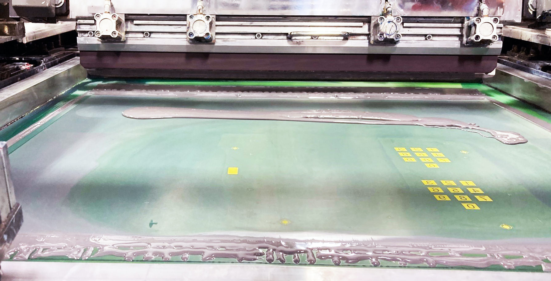
Screen Printing

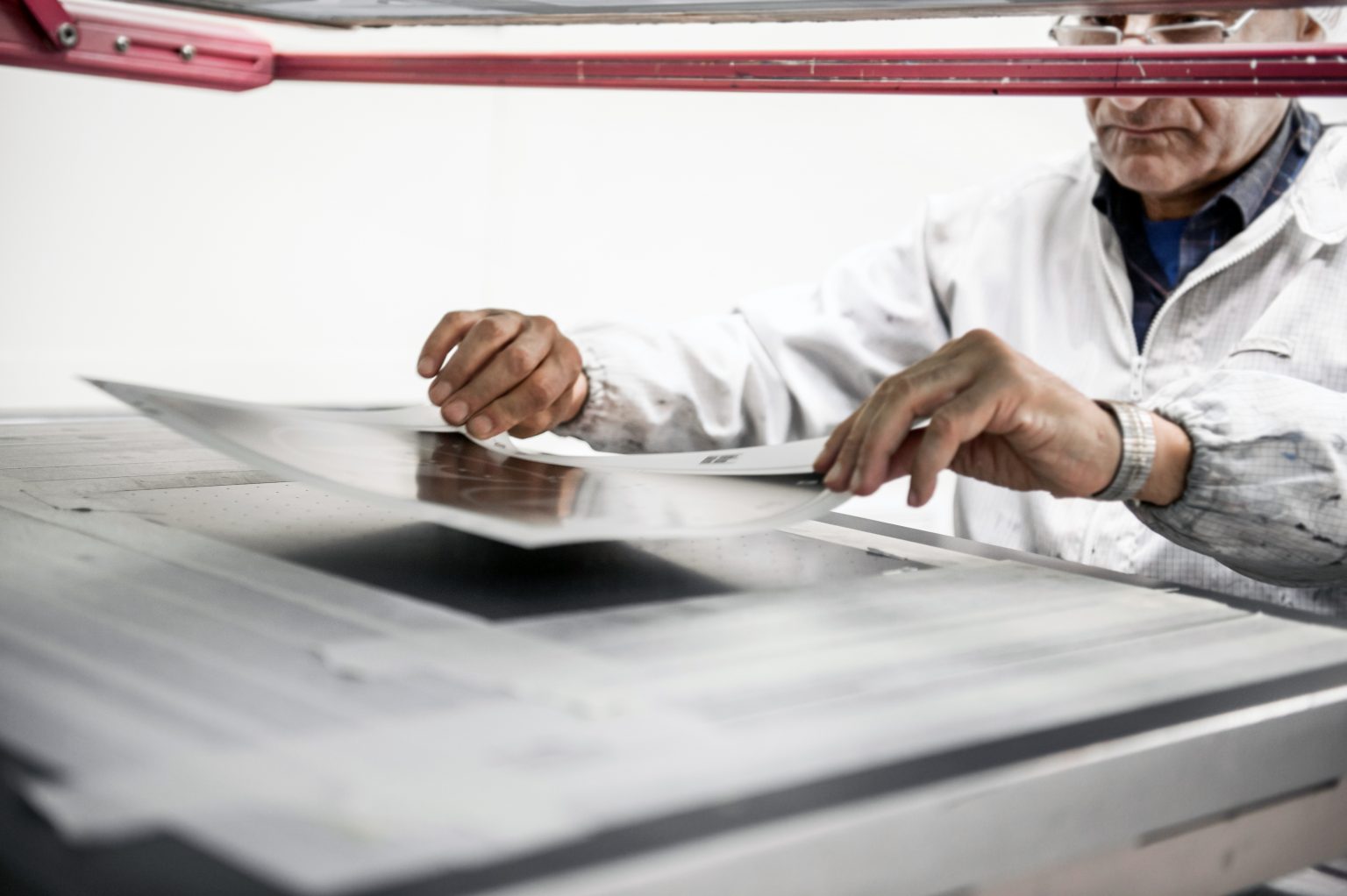
HMI and Printed Electronics

e2ip started as a family business specializing in screen printing, 30 years ago. It began as our main focus and served as an eventual catalyst for establishing and expanding our expertise and leadership in other areas such as printed electronics technologies. In this way, screen printing is our richest and longest standing area of expertise. To this day we have three manufacturing sites where screen printing is carried out daily. Over the years a combination of scientific research and strategic acquisitions have also allowed us to innovate and evolve within the realm of screen printing, establishing entirely new methods and applications that set us apart from competitors.

Screen printing is an additive manufacturing process, whereby images are printed using porous mesh screens and ink. When it comes to HMI and printed electronics, the ink used is a conductive, electrically functional ink, and the substrates we print onto are highly flexible and range widely to best suit the application at hand. Sensors, heaters, actuators, and many other components used in final HMI assemblies are manufactured in this way.

The intricate, conductive patterns deposited onto the substrate form the basis of the electronic functionalities of the final assembly. In this way, screen-printed electronic components have the advantage of being devoid of wires and bulky circuit layers that can corrode and encounter wear and tear that shorten the life of the end product. Lightweight, streamlined components allow for lightweight, streamlined assemblies, that are affordable to produce, robust, and are long-lasting.

Since today the substrate selection is essentially unlimited, surfaces themselves become the substrates. Surfaces become more functional, in smarter ways with bespoke yet highly scalable, affordable production methods.

Where resolution can traditionally be lower in screen printing than in other types of electronics printing methods, e2ip uses a fine line printing method and proprietary inks featuring sub-micron trace thicknesses, that allow for finer lines than can be achieved by competitors. This method is used for printed antennas, for example.

Applications and Features

Key Features

  • Various conductive inks available
  • Compatible with a wide variety of substrates
  • Fine Line printing
  • Flexible substrates
  • Lightweight
  • Energy efficient

Industries

  • Aviation
  • Medical
  • Military
  • Automotive

Applications

  • Printed electronics
  • Membrane switches
  • 5G Smart surfaces
  • Flexible PTC heaters

Learn More

Download the datasheet for our Tamper Proofing Circuits or our Silver Ink Flexible Circuits to see full technological specifications including electrical, mechanical, environmental and certifications.

Electronics should not get in the way of design freedom.

For more information, contact our team.