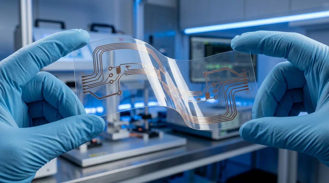
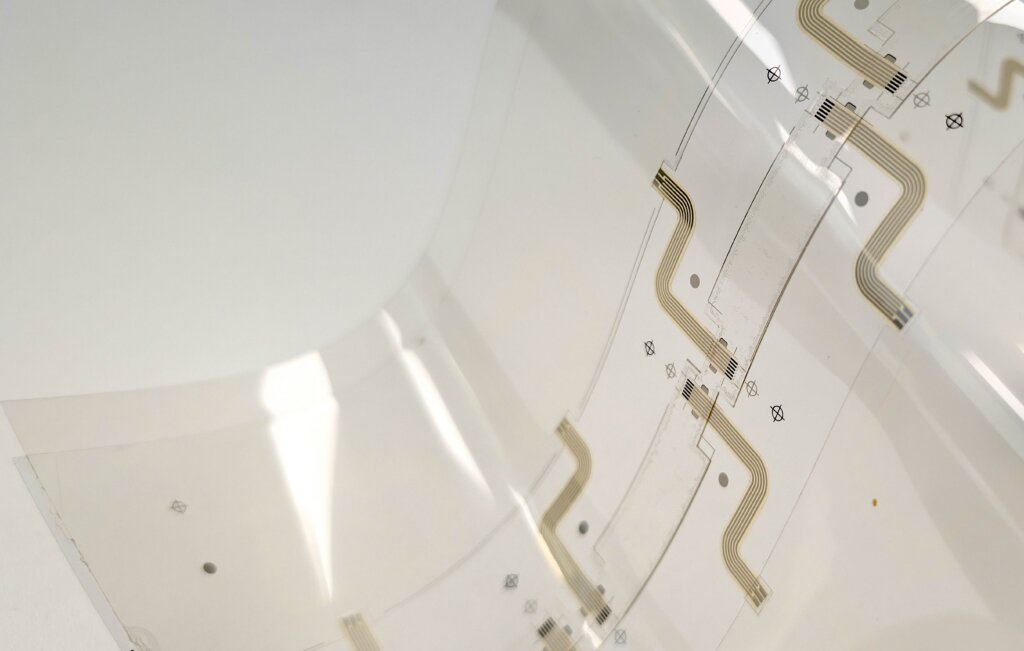
Electronics that are not limited to rigid boards or bulky enclosures, but can instead be thin, flexible, and printed directly onto surfaces much like ink on paper. Circuits can become as lightweight and adaptable as the materials they’re built on, opening new possibilities for product design and manufacturing.
Printed electronics are reshaping how companies think about integrating electronic functionality into everyday products. From next-generation medical devices to smarter automotive interiors and thinner consumer products, this technology offers a practical way to reduce weight, save space, and lower production costs without limiting design flexibility.
What Are Printed Electronics?
Printed electronics are electronic circuits and components created using printing techniques rather than traditional fabrication methods. Instead of removing copper from a rigid board through etching, conductive inks are deposited directly onto flexible substrates such as polyester (PET), polycarbonate, or polyimide film.
This makes printed electronics an additive process, so rather than starting with excess material and cutting away what is not needed, the circuit is built only where functionality is required. The result is a circuit that can be thin, lightweight, and flexible.
These qualities make printed electronics especially valuable in products where traditional printed circuit boards may be too rigid, bulky, or limiting. Printed electronics can conform to different shapes and surfaces, allowing engineers and designers to integrate functionality in places that were previously difficult or impossible.
The term “printed electronics” covers a broad range of technologies, including printed circuits, sensors, heaters, lighting elements, and in-mold electronics (IME). Each application relies on the same core idea: using specialized inks and precise printing methods to add electronic functionality directly onto a surface.
How Do Printed Electronics Work?
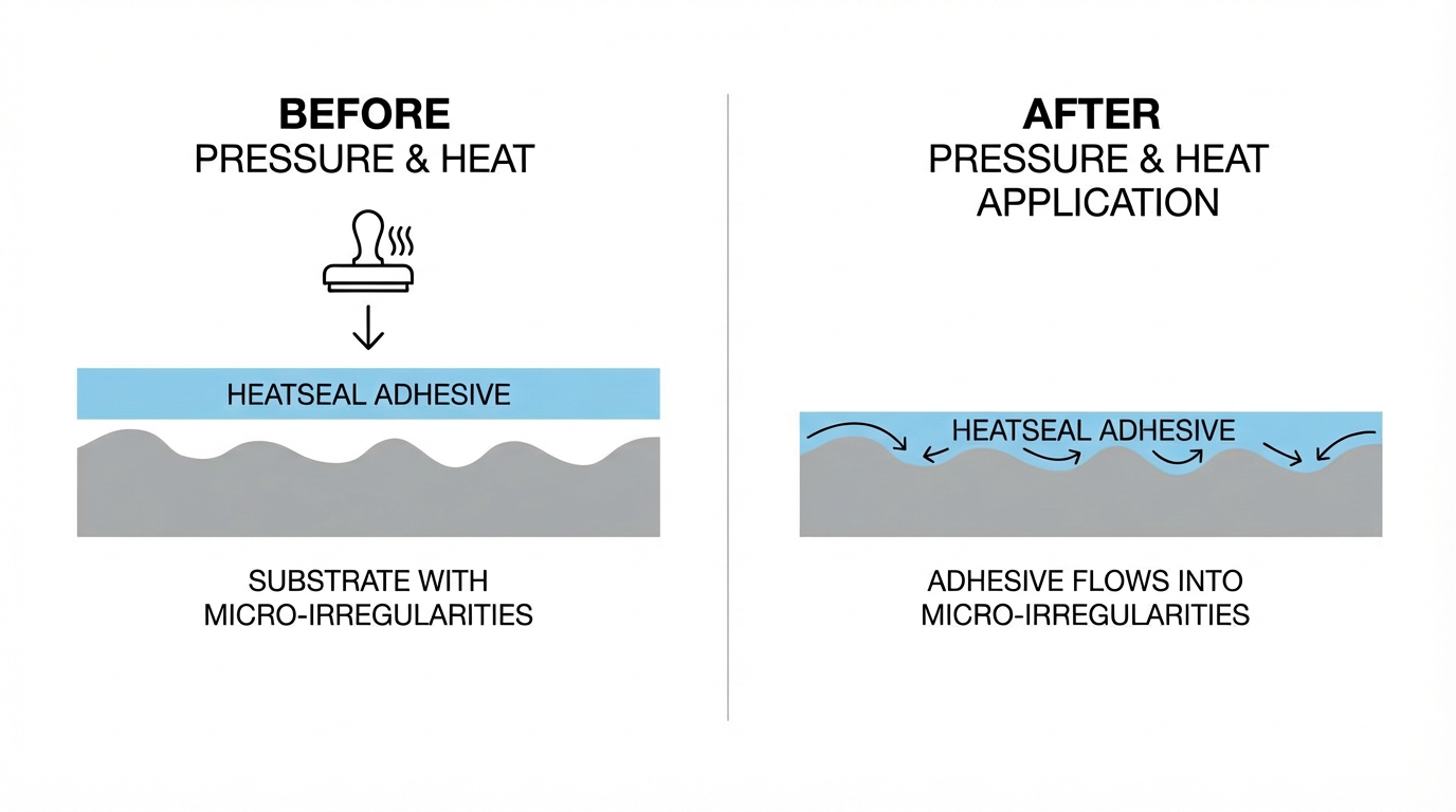
One of the most common production methods is screen printing. Adapted from traditional graphic printing, this process uses a fine mesh screen to transfer conductive ink onto a substrate surface in a precise pattern. Once printed, the traces are cured to achieve the electrical conductivity needed for the application.
The inks are central to the performance of printed electronics. Conductive inks made with silver, carbon, or advanced molecular formulations carry electrical signals in much the same way copper traces do on a conventional circuit board.
One example is MINK molecular ink, a patented, particle-free silver ink developed for high-performance printed electronics. Its strong conductivity and thin profile make it especially useful for applications that require thermoforming into complex 3D shapes. This is critical for in-mold electronics, where printed circuits are molded directly into curved surfaces such as automotive dashboard controls, appliance panels, or control interface surfaces. Printed electronics support everything from prototype development to high-volume manufacturing, allowing companies to produce consistent, precise electronic components at scale.
Why Are Printed Electronics Beneficial?
Printed electronics offer more than a new way to manufacture circuits. They help solve real design, engineering, and production challenges.
Thinner and lighter products
- Printed circuits can be much thinner than traditional PCBs, helping reduce the size and weight of finished products. This is especially valuable in aerospace, automotive, medical, and wearable applications, where every millimeter and gram can matter.
Greater design freedom
- Because printed electronics can be applied to flexible substrates, they can be integrated into curved surfaces, molded parts, textiles, and compact assemblies. Designers are no longer restricted to fitting rigid rectangular boards inside a product. Instead, electronics can become part of the product’s form.
Cost-effective production
- The additive printing process uses material only where it is needed. This reduces waste and can lower production costs compared to conventional copper etching and assembly methods.
Improved integration
- Printed electronics can combine multiple functions into a single thin, flexible layer. Sensors, heaters, touch controls, antennas, lighting, and circuits can be integrated directly into a product surface, reducing the need for separate components and complex assemblies.
More sustainable manufacturing
- By using less material, reducing waste, and supporting lightweight product designs, printed electronics can help reduce environmental impact. As companies face growing pressure to improve sustainability, these advantages are increasingly important.
How Can e2ip Technologies Help?
Printed electronics are only as effective as the expertise behind them and that is where e2ip technologies can provide value. With more than 30 years of screen printing experience and a strong foundation in innovation, e2ip has become a recognized leader in printed electronic solutions for aerospace, medical, defense, automotive, industrial, and consumer markets.
In collaboration with the National Research Council of Canada (NRC), e2ip pioneered MINK molecular ink, a patented innovation designed to overcome the limitations of traditional conductive inks. Its benefits standout with applications that require 3D shaping, thermoforming, or integration into molded surfaces.
e2ip’s printed electronics offerings include:
- Advanced screen printing with fine-line precision, including traces as narrow as 0.050 mm.
- Flexible and stretchable printed heating elements, ideal for curved surfaces.
- Printed sensors for force measurement, occupancy detection, touch input, and medical diagnostics.
- Tamper-proof circuits for high-security applications in banking and defense.
- In-mold electronics for thermoformed 3D surfaces and integrated user interfaces.
What sets e2ip apart is its collaborative approach. The team works closely with OEMs and product development teams to integrate printed electronics into both new and existing products. The goal is to improve performance, reduce weight, lower costs, and enable designs that are difficult to achieve with conventional electronics.
From early concept development through engineering, prototyping, and high-volume manufacturing, e2ip serves as a single-source partner. This helps simplify the path from idea to finished product while ensuring the printed electronics are designed for both performance and manufacturability.
Ready to Rethink What’s Possible?
The move toward printed electronics is already underway. As products become thinner, lighter, smarter, and more integrated, printed electronics offer a proven and scalable way to meet those demands.
Whether you are exploring printed electronics for the first time or looking to improve an existing product, e2ip technologies has the materials expertise, engineering support, and manufacturing capabilities to help bring your vision to life.
Learn more about printed electronics by reaching out to e2ip technologies today.
FAQ
What are printed electronics?
- Printed electronics are circuits and electronic components made by depositing conductive inks onto flexible substrates using printing methods instead of traditional rigid circuit boards. They enable thin, lightweight, and flexible electronic functionality integrated directly onto surfaces.
How do printed electronics work?
- Specialized conductive inks (silver, carbon, or molecular formulations) are printed in precise patterns, commonly via screen printing onto films like PET or polyimide and then cured to form conductive traces and components.
What are the main benefits of printed electronics?
- They reduce weight and thickness, allow electronics to conform to curved or flexible surfaces, lower material waste and cost through additive manufacturing, and enable multifunctional, integrated designs such as sensors, heaters, and touch interfaces.
Where are printed electronics used?
- Common applications include wearable and medical devices, aerospace and automotive interiors (in-mold electronics), smart packaging, sensors and heating elements, and consumer products where space, weight, or form-factor are critical.
How can a company get started with printed electronics?
- Begin by identifying where flexibility, weight reduction, or surface integration would add value; consult with a printed-electronics partner like e2ip for prototyping and material selection; and plan for design-for-manufacturing to scale from prototype to production.