Introduction
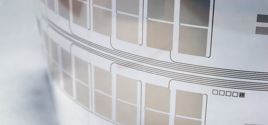
e2ip products are at the forefront of printed electronics and as the demand for smaller, more functional, and aesthetically pleasing electronic devices grows, the need for innovative materials and manufacturing techniques becomes increasingly important. e2ip utilizes a variety of conductive inks such as nanoparticle inks, flake inks, including their patented molecular ink (MINK), developed in collaboration with the National Research Council of Canada (NRC).
Their team is committed to providing optimal solutions for each application by determining the most suitable ink selection based on the design requirements and rheological properties. By leveraging the unique properties of each ink type, e2ip products offer unparalleled functionality, adhesion, durability, and performance in the printing process, making this technology an ideal choice for a wide range of electronic applications. This commitment is further exemplified through the use of molecular inks and their role in smart structural surfaces, where they enable seamless integration of electronics into complex, functional designs.
The Innovation Behind e2ip’s Molecular Ink
Conductive inks are engineered by binding polymers and conductive materials, resulting in inks that deliver high electrical conductivity, flexibility, and formability. Unlike traditional flake inks, e2ip’s MINK is based on ionic molecules, offering superior conductivity, elongation, and compatibility with a wide range of printing techniques such as screen printing and inkjet printing. This innovation, developed in collaboration with the National Research Council of Canada (NRC), addresses the limitations of conventional inks.
Key Benefits of Molecular Ink:
- High Electrical Conductivity: Ensures reliable performance in demanding electronic applications.
- Formability and Flexibility: Allows for seamless integration into curved and freeform surfaces, supporting advanced design freedom, during the thermoforming process.
Enabling SMART STRUCTURAL SURFACES™
SMART STRUCTURAL SURFACES ™ represent a leap in human-machine interface (HMI) design by embedding electronics directly into the structure of surfaces. This methodology eliminates the need for bulky control panels and tech boxes, enabling sleek, lightweight, and highly functional products.
SMART STRUCTURAL SURFACES™ are used in a variety of sectors, from automotive interiors and aircraft armrests to medical devices and home appliances. They enable intuitive, touch-based controls and seamless integration of lighting, sensors, and antennas, all within a single, lightweight unit. This not only improves user experience but also supports space and weight savings and cost-effectiveness.
How Molecular Ink Enable SMART STRUCTURAL SURFACES™:
- Printed Electronics as the Core: The electronic circuitry in SMART STRUCTURAL SURFACES™ is printed using e2ip’s conductive ink, reducing the number of parts and overall device size.
- Design Freedom: The flexibility and formability of the ink allows electronics to be integrated into curved, freeform surfaces, supporting ergonomic and minimalistic designs while maintaining printing quality.
- Streamlined Manufacturing: The ink’s compatible nature with various printing and forming techniques simplifies assembly and reduces costs.
- Aesthetic and Functional Integration: By embedding electronics into the surface, designers can create products that are both visually appealing and highly interactive, with improved touch performance and ease of cleaning.
Conclusion
e2ip’s molecular ink is a foundational technology that enables the creation of SMART STRUCTURAL SURFACES™, redefining what is possible in product design and human-machine interaction. By combining high performance, flexibility, and sustainability, the ink empowers manufacturers to deliver the next generation of intelligent, integrated, and aesthetically pleasing products.
For more information, visit e2ip’s Molecular Ink and SMART STRUCTURAL SURFACES™.