As printed electronics become integrated into industrial and commercial products and solutions, the term ‘printed electronics’ is now mainstream. While leveraging printed electronics, e₂ip technologies, has been working in partnership with the National Research Council of Canada (NRC) to advance the material science and manufacturing of In-Mold Electronics. This article offers an overview of these technologies.
In-Mold Electronics is becoming a common buzzword in the human machine interface (HMI) industry. Understanding the intricacies between the design and the process of producing a finished IME product is not that common, therefore a simplified explanation will help to understand the benefits of the technology.
When the circuit and graphic designs are completed the actual manufacturing processing steps begin. The first process step is the printing phase which requires understanding the ink chemistries and print layer stack-ups. In some cases, the overall print stack-up is completed on a single film and in others two films are used.
The second process step includes the pick-and-place of components required to add LED’s, passive components and in some cases microprocessor capabilities. It should be noted that depending on the types of ink used, the pick-and-place step could move to a later point in the process.
The third process step converts the flat printed sheet to its intended 3D user interface shape. All inks along with the components on the film end up being positioned exactly where intended in the final shape of the part. Typical thermoforming methods include high pressure forming and in some cases vacuum forming. The films are trimmed, sometimes before molding and sometimes after molding, and the circuits are function checked. Molding is the final process consisting of placing the formed films in a mold, where the resin is injected between the films to encapsulate all the components. This also provides the part with its rigid structure and a means for attachment via screw bosses or clips.
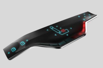
Finished product
From ideation to fabrication, Montreal-based e₂ip Technologies delivers HMI and smart surface solutions to global market leaders.